Low noise amplifier and receiver

a low noise amplifier and receiver technology, applied in the direction gain control, digital transmission, etc., can solve the problem of hard to have the best implementation, and achieve the effect of maintaining increasing the gain compression point (p1db), and improving the linearity of low noise amplifiers

Active Publication Date: 2015-10-01
ADVANCED SEMICON ENG INC
View PDF11 Cites 17 Cited by
  • Summary
  • Abstract
  • Description
  • Claims
  • Application Information

AI Technical Summary

Benefits of technology

[0006]The instant disclosure provides a high linearity low noise amplifier with high P1dB. The low noise amplifier comprises a current mirror circuit, a bias circuit, a cascode amplifying circuit and a power gain compensating circuit. The current mirror circuit provides a first current and a third current according to a system voltage and a preset current, wherein the first current and the third current are mapping current of the preset current. The bias circuit is electrically connected to the current mirror circuit and is used for receiving the first current and outputting a first bias voltage and a second bias voltage according to the first current and the third current. The cascode amplifying circuit is electrically connected to the bias circuit so as to respectively receive the first bias voltage and the second bias voltage, and accordingly to work at an operation bias point. The cascode amplifying circuit is used for receiving and amplifying a RF input signal and accordingly outputs a RF output signal. The power gain compensating circuit is electrically connected between the cascode amplifying circuit and the current mirror circuit. The power gain compensating circuit is used for receiving the RF output signal and accordingly outputting a gain compensating signal to the current mirror circuit so as to dynamically adjust current value of the first current and the third current and further to compensates power gain of the low noise amplifier in order to increase linearity.
[0013]In an embodiment of the instant disclosure, the current mirror circuit further comprises a second feedback resistor. One terminal of the second feedback resistor is connected to gate of the seventh transistor, and another terminal of the second feedback resistor is connected to gate of the fifth transistor. The current value of the source current of the seventh transistor may be increased through ratio of resistor value between the first feedback resistor and the second feedback resistor, so that current value of the first current and third current may be correspondingly increased for increasing 1 dB gain compression point (P1dB) of the low noise amplifier.
[0014]In an embodiment of the instant disclosure, when power of the RF input signal is smaller than a power threshold value, the first transistor and third transistor work at linear region so as to maintain linearity of the low noise amplifier; when power of the RF input signal is larger than a power threshold value, the first transistor and third transistor enter into saturation region from linear region and the first current increases according to increasing of alternative current (ac) component of gate voltage of the sixth transistor, so as to increase voltage value of the first bias voltage and the second bias voltage and further compensate power gain of the low noise amplifier.

Problems solved by technology

There are many bandwidths and communication protocols for mobile network, wide area network (WAN), local area network (LAN), public safety communication and military communication, which is hard to have the best implementation.

Method used


Image

  • Low noise amplifier and receiver
  • Low noise amplifier and receiver
  • Low noise amplifier and receiver

Examples


Embodiment Construction

[0026]It will be understood that, although the terms first, second, third, and the like, may be used herein to describe various elements, components, regions, layers and / or sections, these elements, components, regions, layers and / or sections should not be limited by these terms. These terms are only to distinguish one element, component, region, layer or section from another region, layer or section discussed below could be termed a second element, component, region, layer or section without departing from the teachings of the instant disclosure. As used herein, the term “and / or” includes any and all combinations of one or more of the associated listed items.

[0027]In the following instruction, embodiments together with drawings are for illustrating the low noise amplifier and receiver; however, the embodiments are not taken as limitations for the instant disclosure.

[0028][One Embodiment of the Low Noise Amplifier]

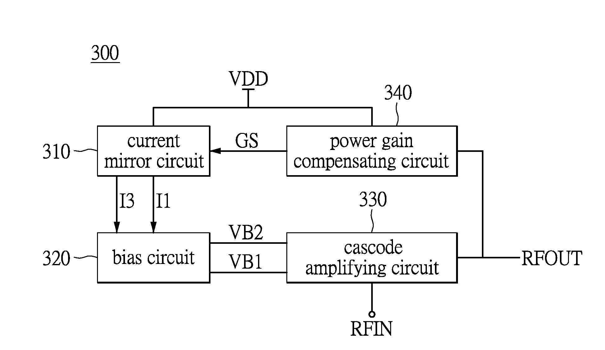
[0029]Please refer to FIG. 3, FIG. 3 shows a schematic block diagram ...


PUM


Abstract

A low noise amplifier is disclosed. The low noise amplifier comprises a current mirror circuit, a bias circuit, a cascode amplifying circuit and a power gain compensating circuit. The current mirror circuit is used for providing a first current and third current. The bias circuit is used for receiving a first current and third current and outputting a first bias voltage and a second bias voltage according to the first current and third current. The cascode amplifying circuit respectively receives the first bias voltage and the second bias voltage, and accordingly to work at an operation bias point. The power gain compensating circuit is used for receiving a RF output signal and accordingly outputs a gain compensating signal to the current mirror circuit so as to dynamically adjust current value of the first current and third current and further to compensates power gain of the low noise amplifier in order to increase 1 dB gain compression point (P1dB).

Description

BACKGROUND OF THE INVENTION[0001]1. Field of the Invention[0002]The instant disclosure relates to a low noise amplifier; in particular, to a high linearity low noise amplifier that can dynamically adjust the bias point to achieve high linearity and high P1dB.[0003]2. Description of Related Art[0004]The wireless communication has developed dramatically. Nowadays, there are over 1 billion wireless mobile devices in the world. There are many bandwidths and communication protocols for mobile network, wide area network (WAN), local area network (LAN), public safety communication and military communication, which is hard to have the best implementation.[0005]The Low Noise Amplifier (LNA) is generally used in the communication system, which is used for amplifying weak input signal received from antenna to be a signal with low noise figure. Moreover, the Low Noise Amplifier (LNA) is often configured at the front end of a communication system. Generally speaking, the Low Noise Amplifier (LNA...

Claims


Application Information

Patent Timeline
Patent Type & Authority Applications(United States)
IPC IPC(8): H03G3/30H03F1/02H03F3/19
CPCH03G3/3036H03F3/19H03F3/00H03F2200/451H03F2200/294H03F1/0205H03F1/223H03F3/193
Inventor DING, JAW-MINGMOU, JIA-HONG
Owner ADVANCED SEMICON ENG INC
Why Eureka
Try Eureka