Method and device for producing a lens wafer

a technology of lens and wafer, which is applied in the direction of auxillary shaping apparatus, ceramic shaping apparatus, applications, etc., can solve the problems of increasing the cost pressure of microlenses which are ideally to be produced in mass production, and the difficulty of optically correct production becomes more difficult, and achieves the effect of high production accuracy

Active Publication Date: 2015-10-15
EV GRP
View PDF13 Cites 4 Cited by
  • Summary
  • Abstract
  • Description
  • Claims
  • Application Information

AI Technical Summary

Benefits of technology

[0007]An advantage of this invention is a device and a method for mass production of microlenses with carriers which have high production accuracy, especially an exactly aligned optical axis.
[0009]The invention is based on the idea of aligning the carrier, especially the wafer, during stamping, especially during shaping of the curable fluid relative to the stamping die. In this way in-situ alignment is enabled. This furthermore has the positive consequence that the distance D between the die and the carrier, especially towards the end of shaping of the microlens field, is as small as possible. In this way the alignment can be done much more precisely than in the prior art.
[0016]According to one embodiment of the invention, the wedge fault equalization or the X-Y alignment takes place continuously after a certain value of a distance D of the stamping side of the wafer and the stamping side of the die is no longer reached. This is because it is especially advantageous to carry out alignment briefly before the stamping or curing of the lens wafer, since at this instant, the distance D between the stamping sides is the minimum possible so that especially with a position detection means which is rigid to the stamping sides extremely accurate detection of the position of the stamping sides and thus the position of the wafer and the die is enabled. Detecting the position of the wafer and of the die or of the respective stamping sides to one another enables exact control of the wedge fault equalization means and of the X-Y alignment by X-Y alignment means.
[0017]Accordingly, it is especially advantageous when shaping according to one embodiment of the invention takes place position-controlled.
[0018]For wedge fault equalization and / or for X-Y alignment, corresponding alignment marks are provided in the die, especially on its stamping side, preferably at least on one peripheral edge of the die, and in the wafer, especially on its stamping side, preferably at least on one peripheral edge of the wafer, there are corresponding alignment marks. Still more exact detection of the position of the stamping sides can be accomplished when the distance between the position marks is as small as possible, and integrated into the stamping sides, especially flush, by the arrangement of the position marks on the stamping sides. In this way, the accuracy of the position detection is distinctly increased.
[0021]The detection precision is improved or increased by the distance D, between the stamping side of the die and the stamping side of the wafer in the Z direction, being greater than 0 and at the same time smaller than the depth of field region in the Z-direction during the position detection.

Problems solved by technology

The more the microlenses are to be miniaturized, the more difficult their optically correct production becomes, because at the same time the cost pressure for the microlenses which are ideally to be produced in mass production is enormous.
The greatest problem for these microlenses with carriers is the correct alignment of the stamping die relative to the carrier.

Method used


Image

  • Method and device for producing a lens wafer
  • Method and device for producing a lens wafer
  • Method and device for producing a lens wafer

Examples


Embodiment Construction

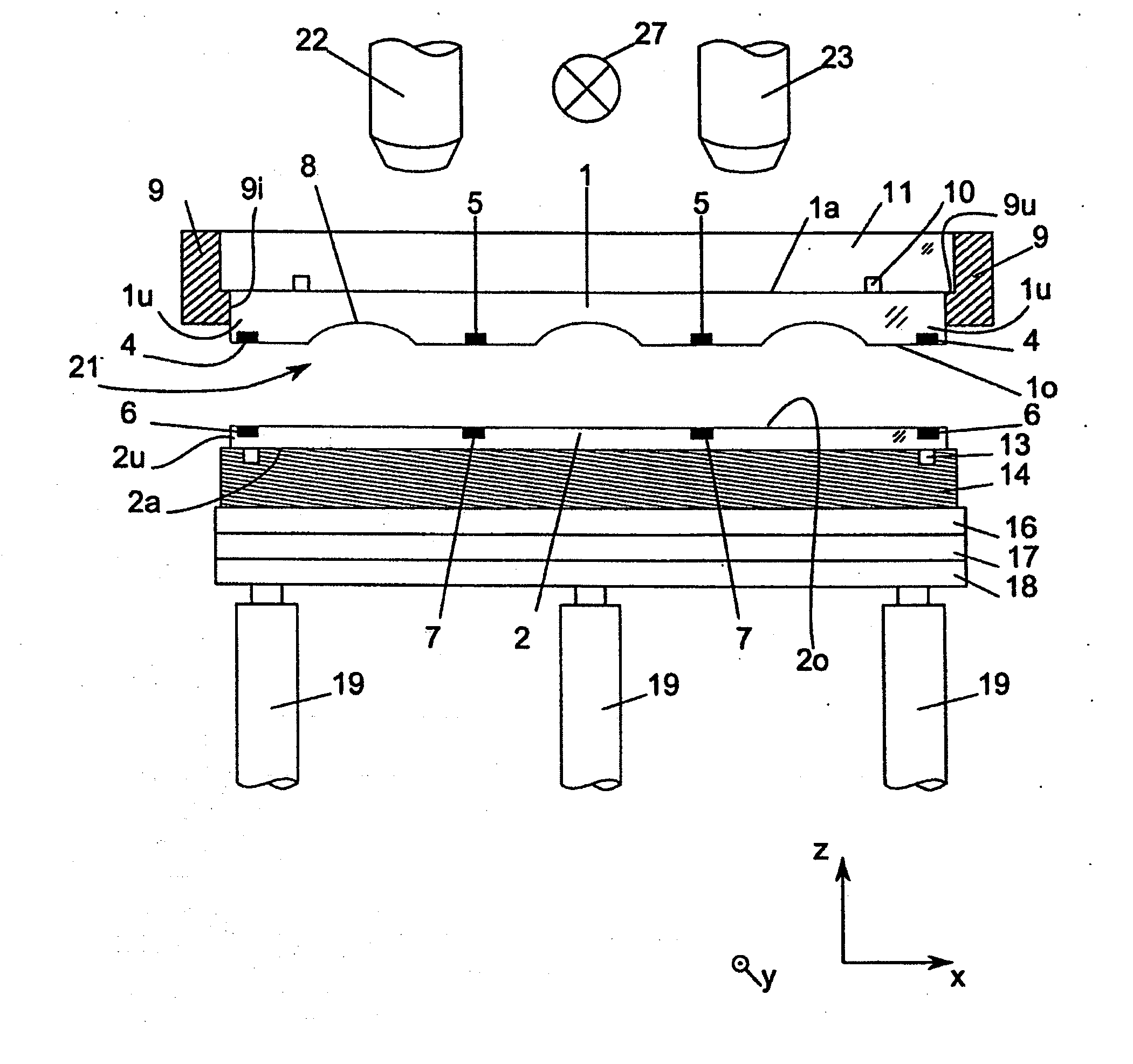
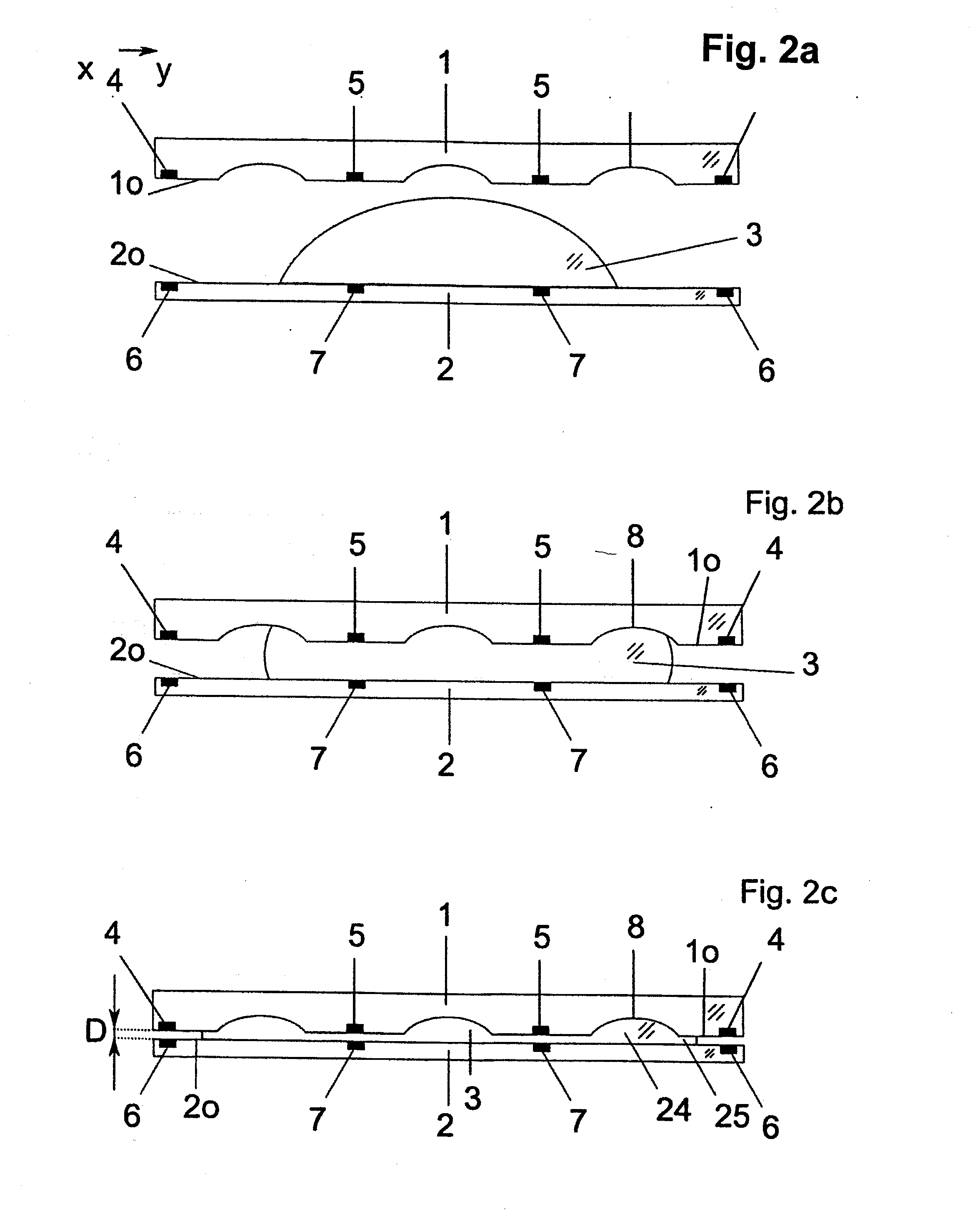
[0043]In the figures the advantages and features of the invention are identified with reference numbers which identify them according to embodiments of the invention, components and features with the same or equivalent function being identified with identical reference numbers.

[0044]FIG. 1 shows a device according to the present invention for producing a lens matrix 25 which has a plurality of microlenses 24 (see FIGS. 2c, 3c and 4c).

[0045]In the embodiments shown, the lens matrix 25 is stamped onto an especially planar wafer 2. A die 1 with one stamping side 1o with a stamping structure 21 which has lens molds 8 is held in a first receiving means. The first receiving means is comprised of a holding device 9 which is ring-shaped on the interior thereof. The holding device 9 includes a peripheral shoulder 9u which extends toward the interior of the ring-shaped holding device. A receiver 11, which is provided with suction paths 10, is inserted and fixed in said holding device 9 on sai...


PUM

PropertyMeasurementUnit
depth ofaaaaaaaaaa
depth ofaaaaaaaaaa
depth ofaaaaaaaaaa

Abstract

A method and a device for producing a lens wafer which has a plurality of microlenses, as well as microlenses produced from the lens wafer.

Description

RELATED APPLICATIONS[0001]This application is a divisional of U.S. patent application Ser. No. 13 / 825,826, filed Mar. 25, 2013, entitled “METHOD AND DEVICE FOR PRODUCING A LENS WAFER,” and claims priority of International Patent Application No. PCT / EP2010 / 006518, filed Oct. 26, 2010, which is fully incorporated herein by reference.FIELD OF THE INVENTION[0002]This invention relates to a method and a device for producing a lens wafer which has a plurality of microlenses. Furthermore, the present invention relates to a lens wafer and microlenses which have been produced from the lens wafer.BACKGROUND OF THE INVENTION[0003]Microlenses are used primarily for devices which require an optical focusing means, such as for example cameras of cell phones. As a result of miniaturization, functional regions will become smaller and smaller. The more the microlenses are to be miniaturized, the more difficult their optically correct production becomes, because at the same time the cost pressure for...

Claims


Application Information

Patent Timeline
Patent Type & Authority Applications(United States)
IPC IPC(8): B29D11/00B29C43/58B29C43/02
CPCB29D11/00365B29C2043/5833B29C43/58B29C43/021B29C33/20B29D11/00278B29D11/005B29D11/00951
Inventor KAST, MICHAELWIMPLINGER, MARKUS
Owner EV GRP
Why Eureka
Try Eureka