Dense PCB (printed circuit board) circuit and manufacturing method

A circuit manufacturing and PCB board technology, applied in printed circuit manufacturing, removal of conductive materials by chemical/electrolytic methods, and printed circuits, etc., can solve the problems of poor PCB circuit accuracy and easy occurrence of open circuits, and improve product quality and Accuracy, avoiding open gaps, and solving the effect of dry film adhesion problems

Inactive Publication Date: 2017-06-13
SHENZHEN KINWONG ELECTRONICS
View PDF4 Cites 5 Cited by
  • Summary
  • Abstract
  • Description
  • Claims
  • Application Information

AI Technical Summary

Problems solved by technology

[0006] In view of the above-mentioned deficiencies in the prior art, the object of the present invention is to provide a fine and dense PCB circuit and a manufacturing method, aiming at solving the problems of poor precision of existing PCB circuits with small line width and line spacing, and prone to open circuits.

Method used


Image

  • Dense PCB (printed circuit board) circuit and manufacturing method
  • Dense PCB (printed circuit board) circuit and manufacturing method
  • Dense PCB (printed circuit board) circuit and manufacturing method

Examples


Embodiment Construction

[0026] The present invention provides a fine PCB circuit and a manufacturing method. In order to make the purpose, technical solution and effect of the present invention clearer and clearer, the present invention will be further described in detail below. It should be understood that the specific embodiments described here are only used to explain the present invention, not to limit the present invention.

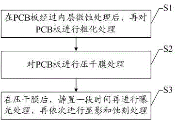
[0027] see figure 1 , figure 1 It is a flow chart of a preferred embodiment of a fine and compact PCB circuit manufacturing method of the present invention, as shown in the figure, which includes steps:

[0028] S1. After the PCB board has undergone micro-etching treatment on the inner layer, roughen the PCB board;

[0029] S2, carry out dry film treatment to PCB board;

[0030] S3. After drying the film, let it stand for a period of time before performing exposure treatment, and then sequentially perform development and etching treatment.

[0031] By improving the trad...


PUM


Abstract

The invention discloses a dense PCB (printed circuit board) circuit and a manufacturing method. The manufacturing method comprises the following steps of A, performing micro-etching treatment on an inner layer of a PCB, and roughening the PCB; B, pressing and drying a film on the PCB; C, standing for a period of time, and exposing; sequentially developing and etching. The manufacturing method has the advantages that the surface of the PCB is roughened, so as to solve the problem of bonding force of the dry film, avoid the open-loop notch, and improve the product quality and precision of a product.

Description

technical field [0001] The invention relates to the field of PCB circuits, in particular to a fine and compact PCB circuit and a manufacturing method. Background technique [0002] Continuously reducing volume, reducing cost, and improving performance are the future development directions of PCB. As an important signal transmission path of PCB, the line width and spacing are limited by its wiring space. In order to save limited space, more components and lines are laid out. The line width and spacing have changed from 6mil (line width) 10 years ago. ) / 6mil (spacing) to the current 3mil / 3mil. [0003] Thin lines and small spacing are hot technologies that PCB suppliers are competing to develop. At present, the PCB industry controls the dimensional tolerance of precision lines above 4mil according to the IPC standard tolerance of ±20%, but for lines / spacings less than 4mil , and also controlled according to the tolerance of ±20%, it seems that the difficulty is greatly incre...

Claims


Application Information

Patent Timeline
Patent Type & Authority Applications(China)
IPC IPC(8): H05K3/06
CPCH05K3/06H05K2203/11
Inventor 陆玉婷王俊李淼徐鹏程
Owner SHENZHEN KINWONG ELECTRONICS
Why Eureka
Try Eureka