Unlock instant, AI-driven research and patent intelligence for your innovation.
Semiconductor device
What is Al technical title?
Al technical title is built by PatSnap Al team. It summarizes the technical point description of the patent document.
a technology of semiconductor devices and semiconductors, applied in semiconductor devices, semiconductor/solid-state device details, electrical apparatus, etc., can solve the problems of unintentional cutting or separation of wires, reducing manufacturing efficiency, and comparatively thin wires, so as to enhance manufacturing efficiency and improve manufacturing efficiency
Active Publication Date: 2015-10-15
ROHM CO LTD
View PDF1 Cites 0 Cited by
Summary
Abstract
Description
Claims
Application Information
AI Technical Summary
This helps you quickly interpret patents by identifying the three key elements:
Problems solved by technology
Method used
Benefits of technology
Benefits of technology
The present invention aims to improve the manufacturing efficiency of semiconductor devices and enhance the reliability of joining the semiconductor element to either a conduction connection member or a heat dissipation member. Therefore, the technical effects of the patent text are to increase the speed and accuracy of semiconductor device manufacturing, as well as to provide more reliable connections between the semiconductor element and other components.
Problems solved by technology
This is thus an impediment to improving the manufacturing efficiency of the semiconductor device.
Also, the wires are comparatively thin, and thus could possibly be unintentionally cut or separate during the manufacturing process of the semiconductor device or use of the semiconductor device.
Method used
Image
Click on the blue label to locate the original text in one second.
Reading with bidirectional positioning of images and text.
Examples
first embodiment
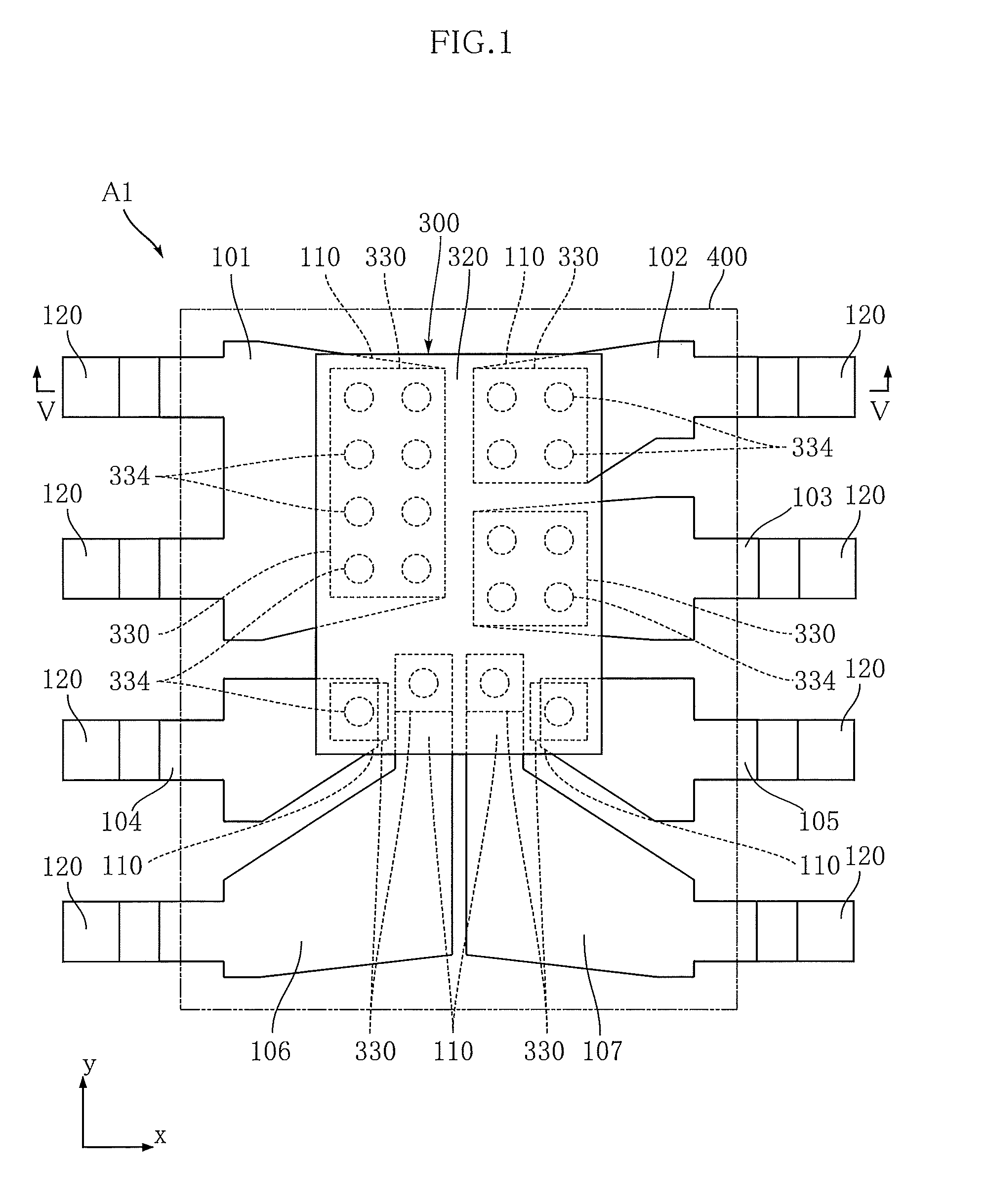
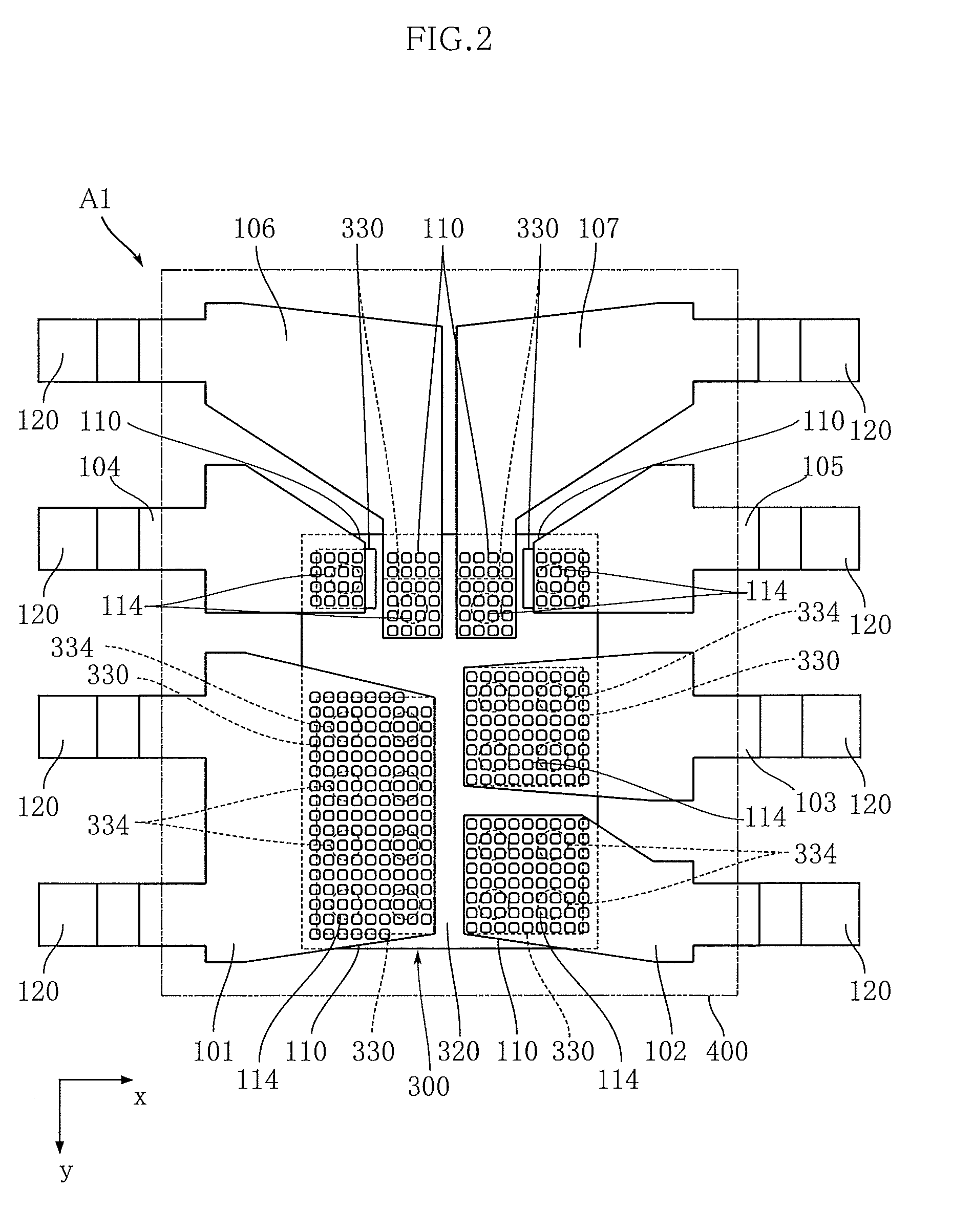
[0135]FIGS. 1 to 6 show a semiconductor device that is based on the present invention. A semiconductor device A1 of the present embodiment is provided with leads 101 to 107, a semiconductor element 300, and a sealing resin 400.
[0136]FIG. 1 is a plan view showing the semiconductor device A1. FIG. 2 is a bottom view showing the semiconductor device A1. FIG. 3 is a front view showing the semiconductor device Al. FIG. 4 is a side view showing the semiconductor device A1. FIG. 5 is a cross-sectional view along a line V-V in FIG. 1. FIG. 6 is an enlarged cross-sectional view showing a main section of the semiconductor device A1.
[0137]The leads 101 to 107 are examples of a conduction supporting member as referred to in the present invention. The leads 101 to 107 constitute conduction paths between the semiconductor element 300 and outside the semiconductor device A1, and support the semiconductor element 300. The leads 101 to 107 are made of a metal, and are preferably made of either Cu or...
second embodiment
[0172]FIGS. 15 to 20 show a semiconductor device that is based on the present invention. A semiconductor device A2 of the present embodiment is provided with leads 101 to 107, a semiconductor element 300, and a sealing resin 400.
[0173]FIG. 15 is a plan view showing the semiconductor device A2. FIG. 16 is a bottom view showing the semiconductor device A2. FIG. 17 is a front view showing the semiconductor device A2. FIG. 18 is a side view showing the semiconductor device A2. FIG. 19 is a cross-sectional view along a line XIX-XIX in FIG. 15. FIG. 20 is an enlarged cross-sectional view showing a main section of the semiconductor device A2.
[0174]The leads 101 to 107 are examples of a conduction supporting member as referred to in the present invention. The leads 101 to 107 constitute conduction paths between the semiconductor element 300 and outside the semiconductor device A2, and support the semiconductor element 300. The leads 101 to 107 are made of a metal, and are preferably made of...
third embodiment
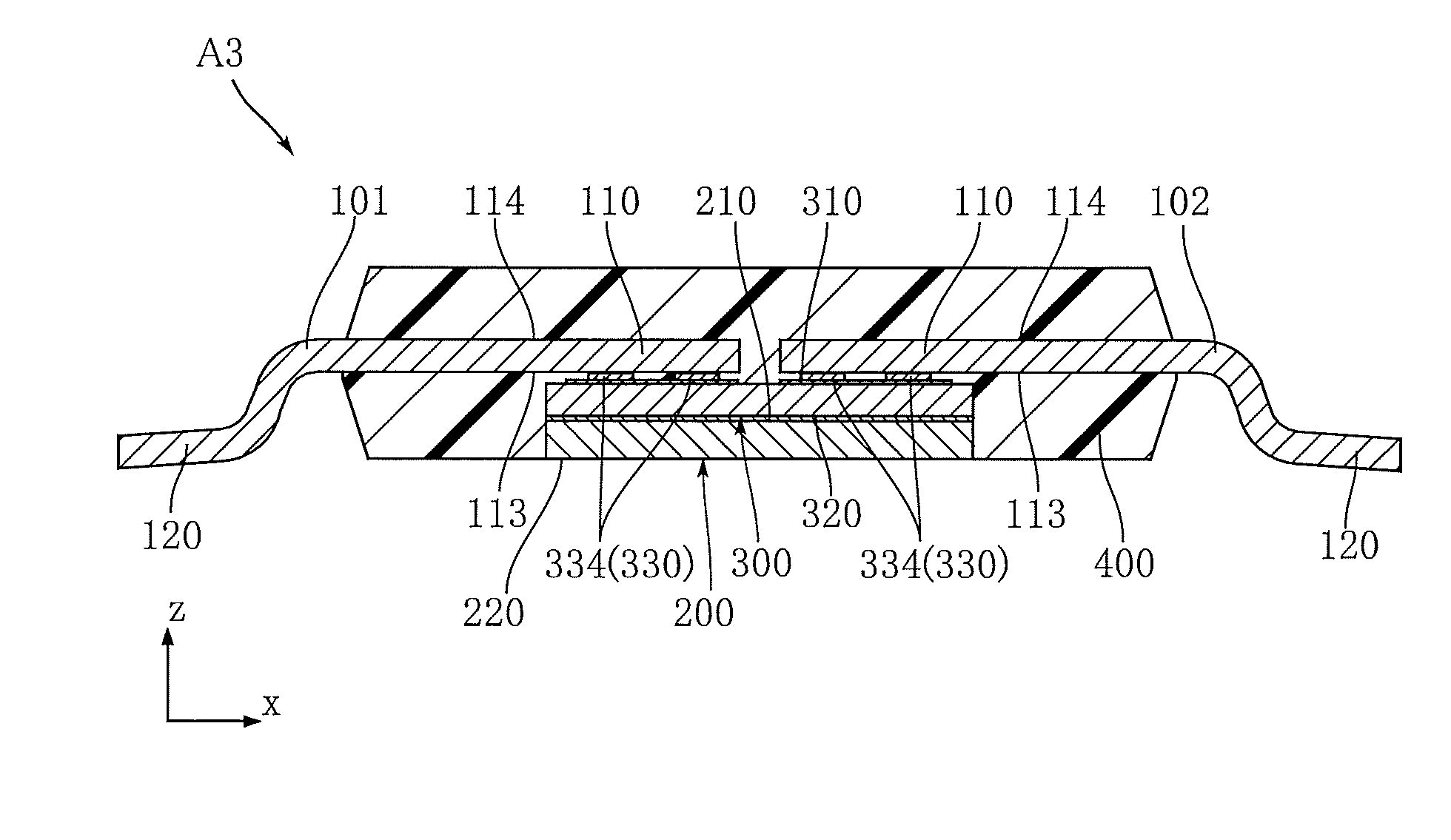
[0197]FIGS. 25 to 30 show a semiconductor device that is based on the present invention. A semiconductor device A3 of the present embodiment is provided with leads 101 to 107, a heat dissipation member 200, a semiconductor element 300, and a sealing resin 400.
[0198]FIG. 25 is a plan view showing the semiconductor device A3. FIG. 26 is a bottom view showing the semiconductor device A3. FIG. 27 is a front view showing the semiconductor device A3. FIG. 28 is a side view showing the semiconductor device A3. FIG. 29 is a cross-sectional view along a line XXIX-XXIX in FIG. 25. FIG. 30 is an enlarged cross-sectional view showing a main section of the semiconductor device A3.
[0199]The leads 101 to 107 are examples of a conduction supporting member as referred to in the present invention. The leads 101 to 107 constitute conduction paths between the semiconductor element 300 and outside the semiconductor device A3, and support the semiconductor element 300. The leads 101 to 107 are made of a ...
PUM
Abstract
A semiconductor device has a semiconductor element provided with a functional surface on which a functional circuit is formed and with a back surface facing in the opposite direction to the functional surface, while also having a lead supporting the semiconductor element and electrically connected to the semiconductor element, and a resin package covering at least a portion of the semiconductor element and the lead. The semiconductor element has a functional surface side electrode formed on the functional surface and equipped with a functional surface side raised part that projects in the direction in which the functional surface faces. The functional surface side raised part of the functional surface side electrode is joined to the lead by solid state bonding.
Description
BACKGROUND OF THE INVENTION[0001]1. Field of the Invention[0002]The present invention relates to a semiconductor device.[0003]2. Description of Related Art[0004]In a semiconductor device having a built-in semiconductor element, a conduction supporting member that constitutes a conduction path to the semiconductor device and supports the semiconductor element is used. In such a semiconductor device, a lead made of a metal is used as the conduction supporting member. A plurality of wires made of Au or the like are used as means for electrically connecting the semiconductor element to the lead. Known documents relating to semiconductor devices include JP-A-2014-7363, for example.[0005]In the manufacturing process of the semiconductor device, a process for bonding the plurality of wires is executed. This bonding process is performed sequentially on the plurality of wires, and cannot be executed collectively on the plurality of wires. This is thus an impediment to improving the manufactu...
Claims
Application Information
Patent Timeline
Application Date:The date an application was filed.
Publication Date:The date a patent or application was officially published.
First Publication Date:The earliest publication date of a patent with the same application number.
Issue Date:Publication date of the patent grant document.
PCT Entry Date:The Entry date of PCT National Phase.
Estimated Expiry Date:The statutory expiry date of a patent right according to the Patent Law, and it is the longest term of protection that the patent right can achieve without the termination of the patent right due to other reasons(Term extension factor has been taken into account ).
Invalid Date:Actual expiry date is based on effective date or publication date of legal transaction data of invalid patent.
Patent Type & Authority Applications(United States)

