Solid-state image sensor, method of controlling the same, electronic device, and storage medium
a solid-state image sensor and image sensor technology, applied in the field of solid-state image sensors and electronic devices, can solve the problems of periodic noise, inability to neglect the impedance between gnds in local gnd connection, and large number of ff elements simultaneously consuming current, so as to achieve the effect of suppressing image quality degradation
- Summary
- Abstract
- Description
- Claims
- Application Information
AI Technical Summary
Benefits of technology
Problems solved by technology
Method used
Image

Examples
first embodiment
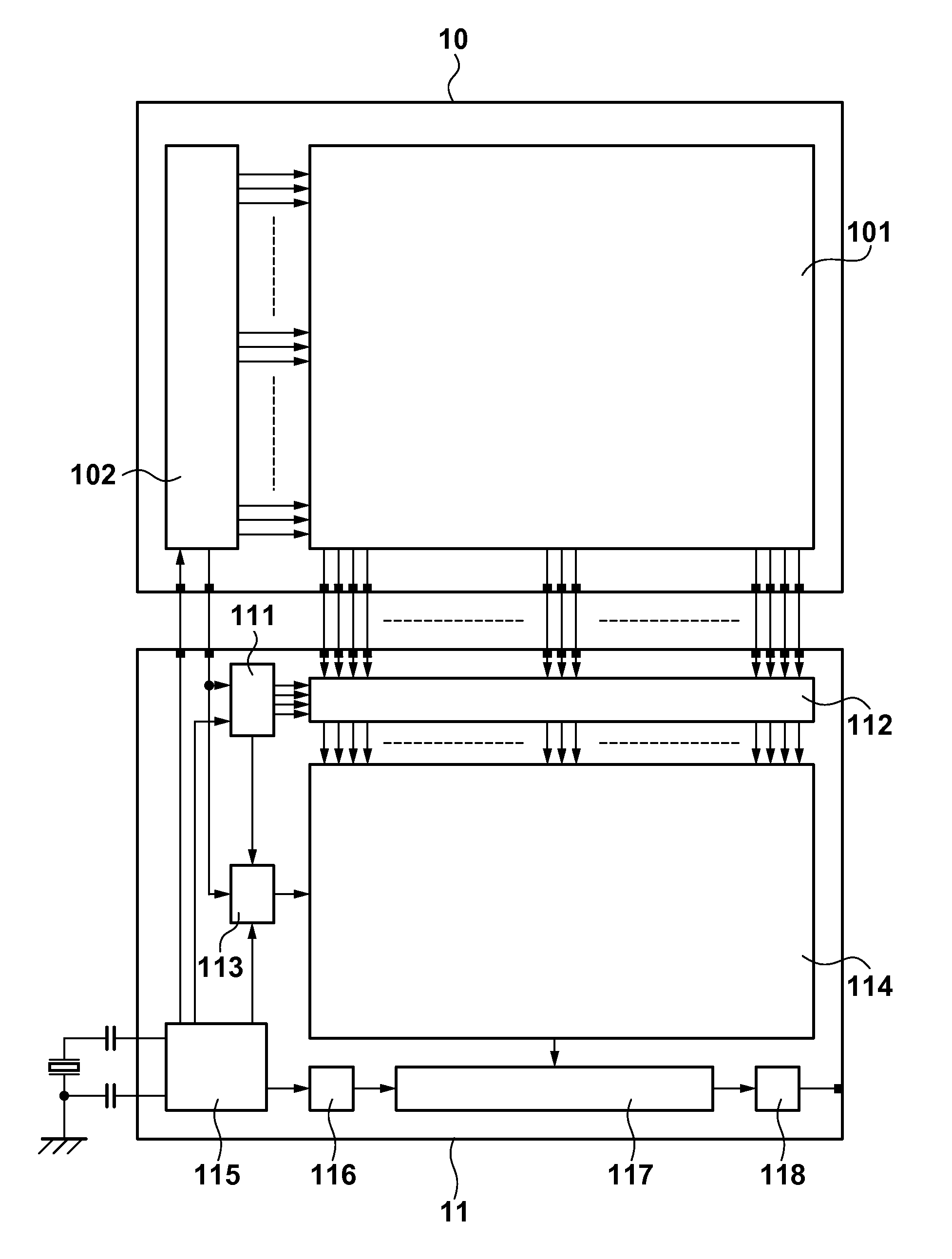
[0031]This embodiment is directed to the structure of a solid-state image sensor. An semiconductor element that implements the image sensor according to this embodiment has a stacked structure of a first semiconductor layer in which an analog signal processing unit such as an imaging pixel portion is implemented and a second semiconductor layer in which a digital signal processing unit is implemented. FIG. 1 is a block diagram showing the arrangement of the image sensor according to this embodiment. An imaging pixel portion 101 is implemented in a first semiconductor layer 10, and a digital signal processing unit 114 is implemented in the second semiconductor layer 11.
[0032]Referring to FIG. 1, a plurality of pixels each including a photoelectric conversion portion and a plurality of transistors are two-dimensionally arrayed in the imaging pixel portion 101. A drive control unit 102 implemented in the first semiconductor layer 10 together with the imaging pixel portion 101 is a circ...
second embodiment
[0049]In the first embodiment, operation control (clock masking processing) of the digital signal processing unit resulting from the operations of imaging pixel portion drive signals (signals sig_301, sig_302, and sig_303 shown in FIG. 3 described above) handled by the drive control unit 102 in FIG. 1 has been described. In this embodiment, operation control (clock masking processing) of a digital signal processing unit resulting from the operations of A / D conversion unit drive signals (signals sig_402 to sig_404 shown in FIG. 3) handled by a drive control unit 111 of an A / D conversion unit 112 in FIG. 1 will be described.
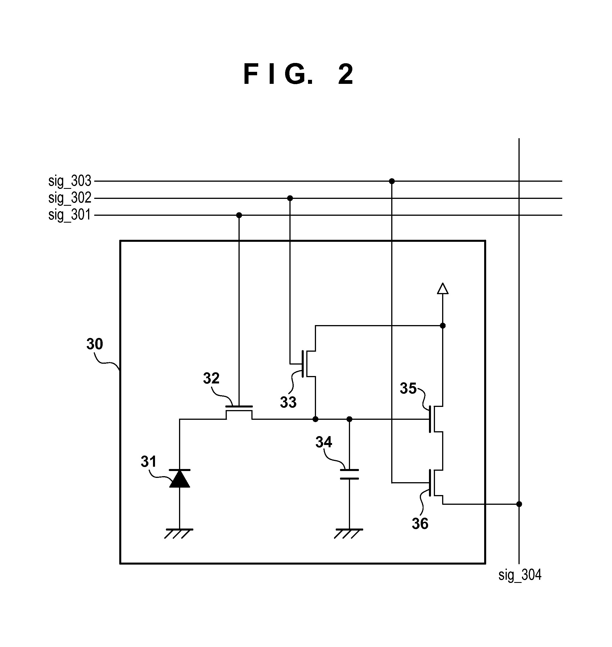
[0050]FIG. 7 is a block diagram showing the relationship between an imaging pixel portion and the A / D conversion unit. The relationship between an imaging pixel portion 101 and a drive control unit 102 in a first semiconductor layer 10 in which the imaging pixel portion 101 is implemented is the same as in the first embodiment. Unit pixels 30 shown in FIG. 2 are tw...
third embodiment
[0077]FIG. 12 is a block diagram showing the arrangement of a portable telephone 2100 (electronic device) according to the third embodiment of the present invention. The portable telephone 2100 according to this embodiment has not only a speech communication function but also an email function, Internet connection function, image shooting and reproduction function, and the like.
[0078]Referring to FIG. 12, a communication unit 2101 communicates speech data or image data to another telephone using a communication method complying with the communication carrier to which the user has subscribed. In speech communication, a speech processing unit 2102 converts speech data from a microphone 2103 into a format suitable for a call and sends it to the communication unit 2101. The speech processing unit 2102 also decodes speech data of the communication partner sent from the communication unit 2101 and sends it to a speaker 2104. An imaging unit 2105 includes an image sensor described in the f...
PUM
 Abstract
Description
Claims
Application Information
 - R&D
- Intellectual Property
- Life Sciences
- Materials
- Tech Scout
- Unparalleled Data Quality
- Higher Quality Content
- 60% Fewer Hallucinations
Browse by: Latest US Patents, China's latest patents, Technical Efficacy Thesaurus, Application Domain, Technology Topic, Popular Technical Reports.
© 2025 PatSnap. All rights reserved.Legal|Privacy policy|Modern Slavery Act Transparency Statement|Sitemap|About US| Contact US: help@patsnap.com