
Shift register unit, gate driving circuit, and display device
- Summary
- Abstract
- Description
- Claims
- Application Information
AI Technical Summary
Benefits of technology
Problems solved by technology
Method used
Image

Examples
Embodiment Construction
[0032]Technical solutions in embodiments of the present invention will be described clearly and completely below in conjunction with the accompanying drawings, and the embodiments to be described are merely a part but not all of the embodiments of the present invention. All other embodiments which, based on the embodiments of the present invention, are obtained by those skilled in the art without creative efforts belong to the protection scope of the present invention.
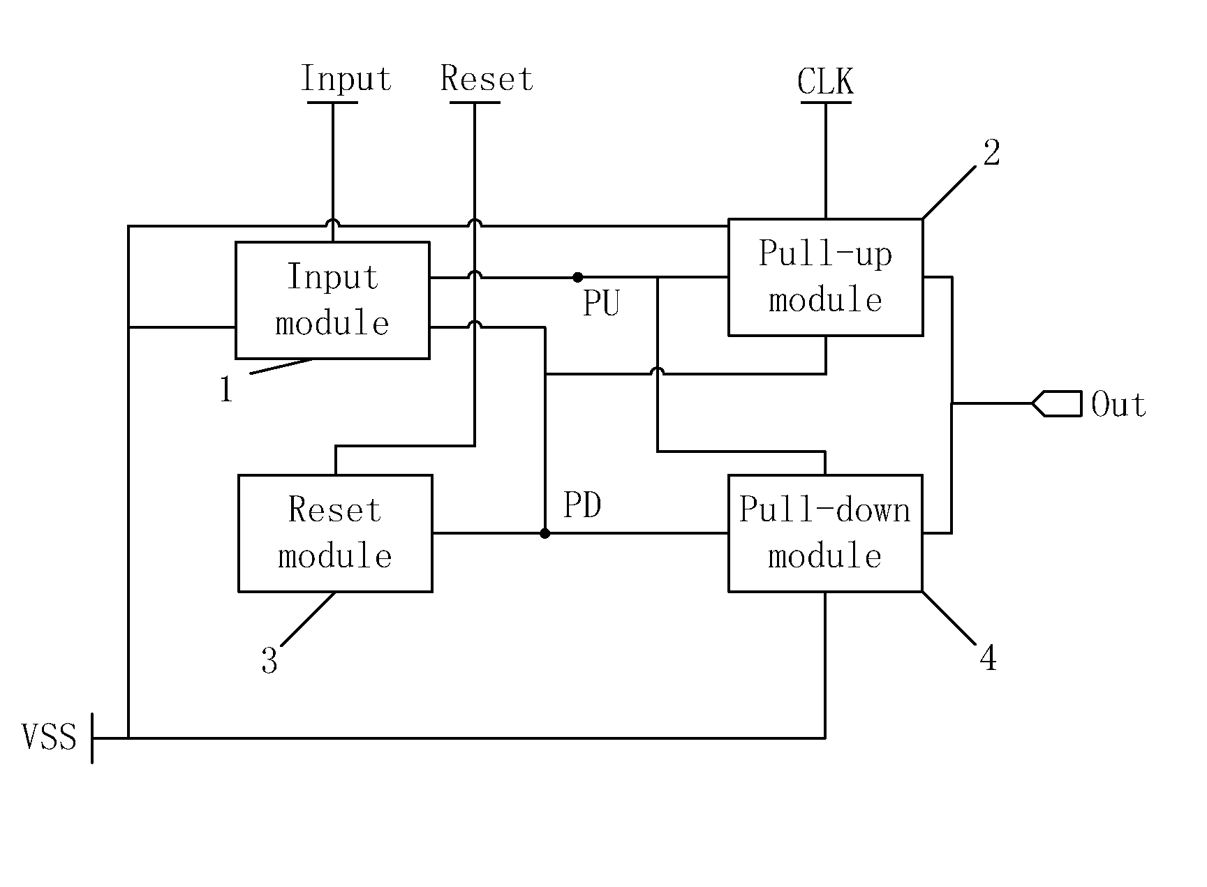
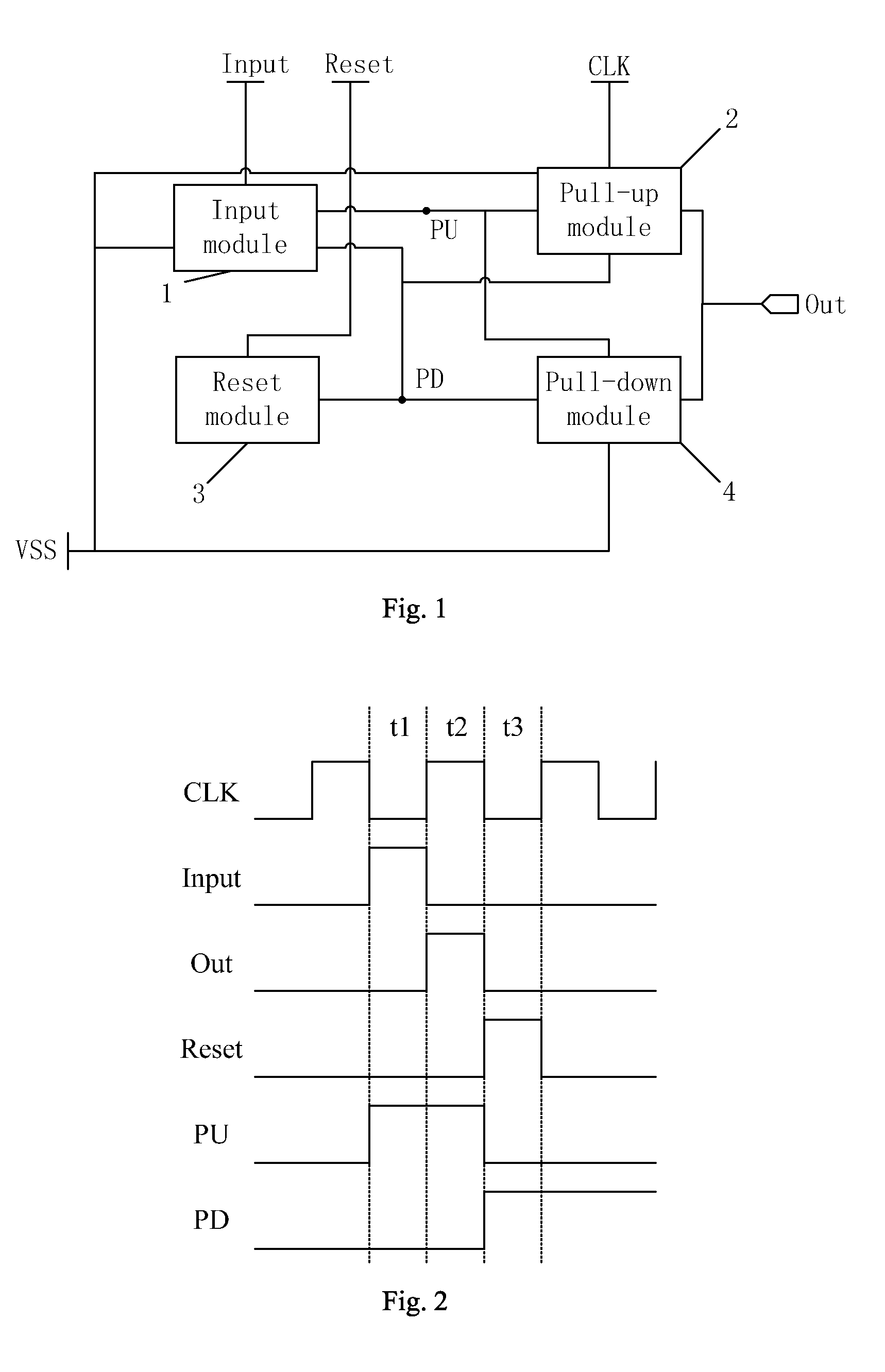
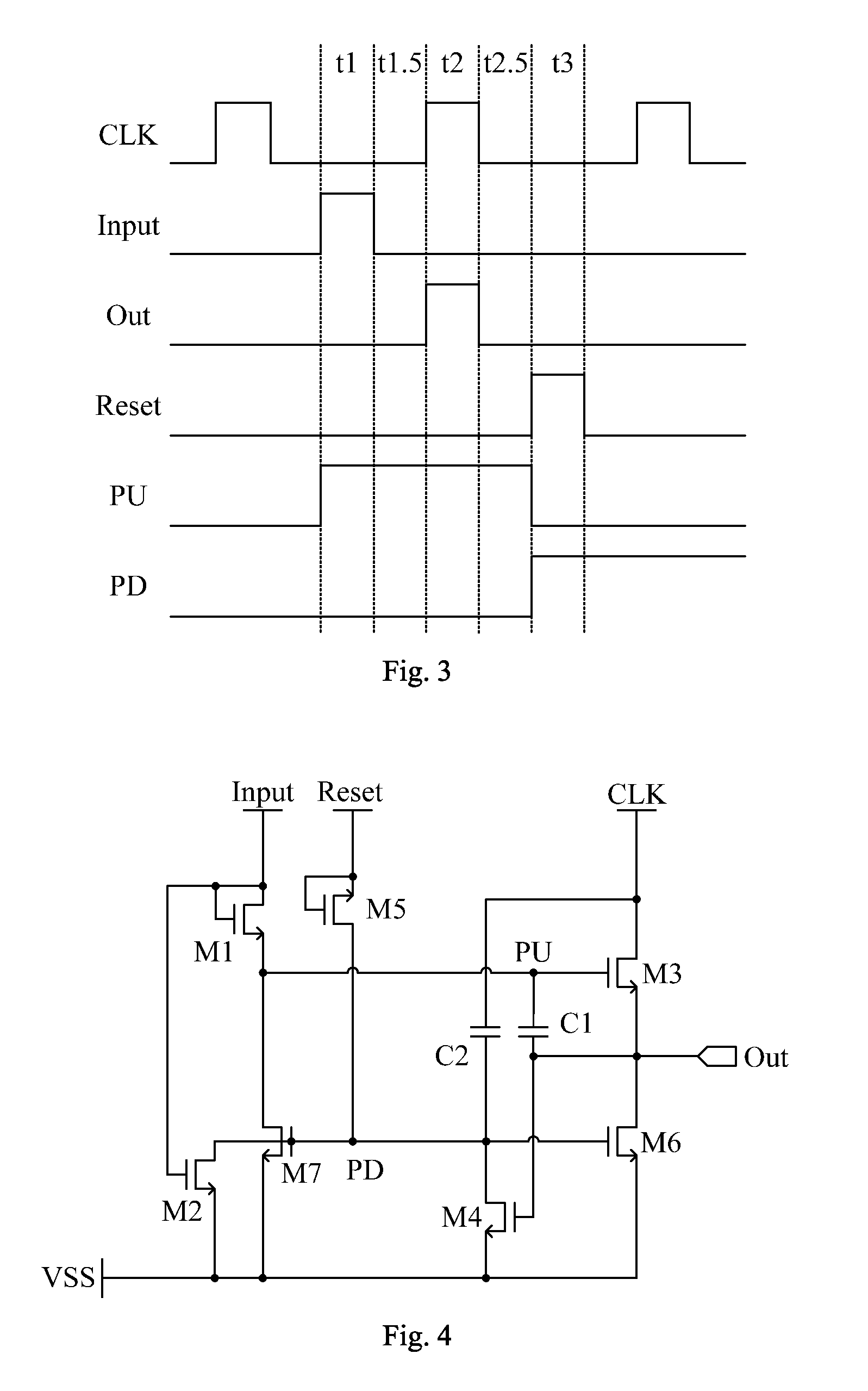
[0033]As shown in FIG. 1, the embodiments of the present invention provide a shift register unit, comprising: an input module 1 connected to a shift register input terminal Input, a first node PU, a second node PD and a turn-off level input terminal VSS, the input module 1 being used for, in response to a turn-on level (that is, a shift register input signal) input via the shift register input terminal Input, providing the turn-on level input via the shift register input terminal Input to the first node PU, and providi...
PUM
 Abstract
Description
Claims
Application Information