

Semiconductor apparatus including a heat dissipating member
- Summary
- Abstract
- Description
- Claims
- Application Information
AI Technical Summary
Benefits of technology
Problems solved by technology
Method used
Image

Examples
embodiment 1
Variation 2 of Embodiment 1
[0121]Here, the semiconductor apparatus according to Variation 2 of Embodiment 1 will be described with reference to FIG. 16A through FIG. 16C. Note that FIG. 16A is a schematic plan view of the semiconductor apparatus according to Variation 2 of Embodiment 1, when the encapsulant is transparent. FIG. 16B is a cross sectional view of the semiconductor apparatus taken at line XVIb-XVIb in FIG. 16A. FIG. 16C is a cross sectional view of the semiconductor apparatus taken at line XVIc-XVIc in FIG. 16A.
[0122]In Variation 2, the spaces formed in heat dissipating member 4 that prevent interference with the regions in which connection member 3 are disposed are provided as openings 4b instead of notched sections 4a. Each opening 4b is provided above a region in which connection members 3 are disposed. With this configuration, since the side surfaces of heat dissipating member 4 are exposed around the entire perimeter of the semiconductor apparatus, the heat dissipa...
embodiment 2
Manufacturing Method
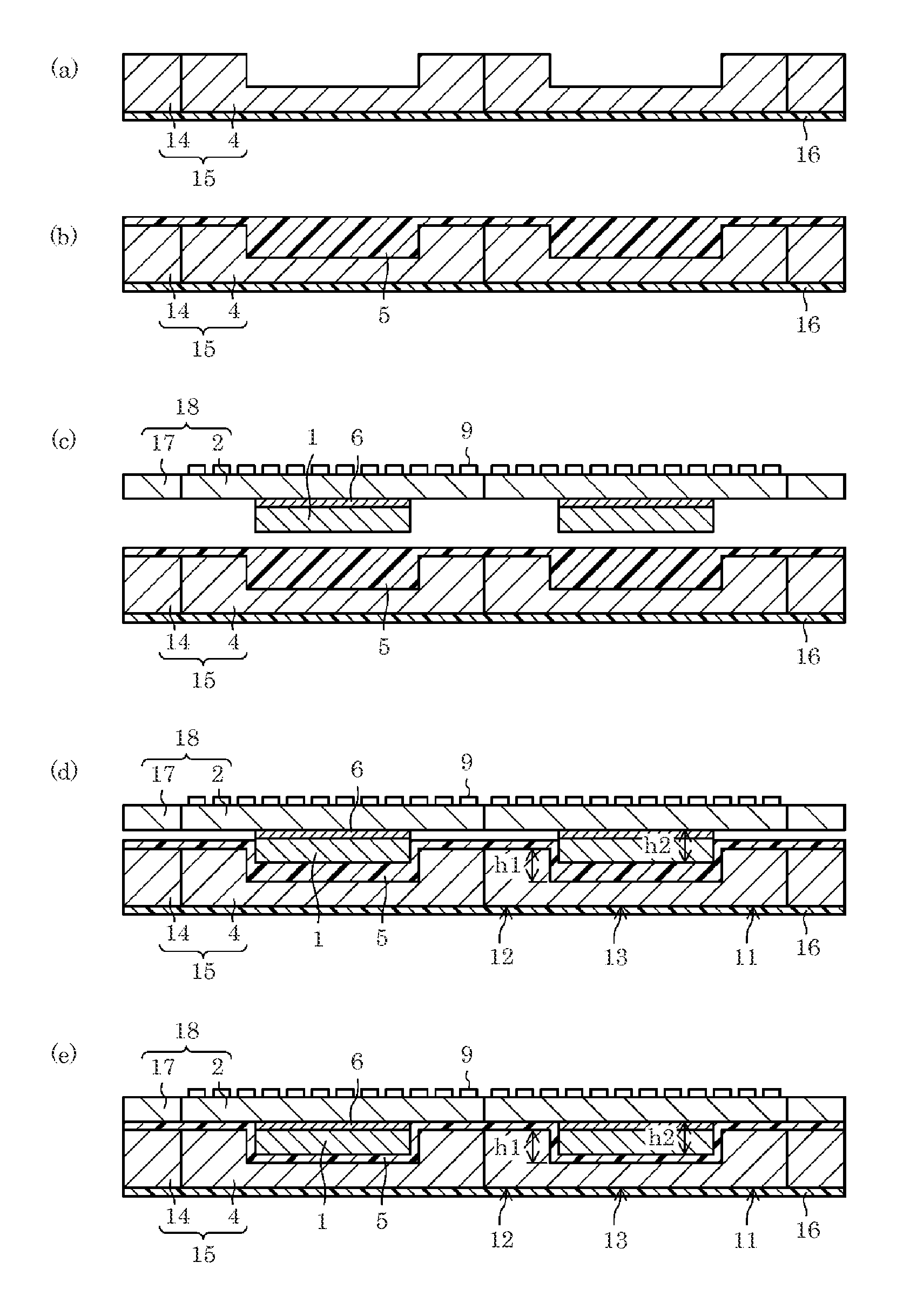
[0138]Next, the method of manufacturing the semiconductor apparatus according to Embodiment 2 will be described with reference to FIG. 20A and FIG. 20B. FIG. 20A is a schematic plan view of the heat dissipating member frame in a manufacturing process of the semiconductor apparatus according to Embodiment 2. FIG. 20B is a cross sectional view of the semiconductor apparatus taken at line XXb-XXb in FIG. 20A.
[0139]Similar to the manufacturing method according to Embodiment 1, the method of manufacturing the semiconductor apparatus according to Embodiment 2 includes using base frame 18 and heat dissipating member frame 15 and collectively encapsulating base 2 and heat dissipating member 4 arranged in a matrix. Manufacturing processes include a frame bonding process including bonding together base frame 18 and heat dissipating member frame 15, a die bonding process including mounting each semiconductor device 1 on a corresponding one of bases 2, a wire bonding process...
PUM
 Abstract
Description
Claims
Application Information