Light emitting device and fabrication method thereof

a technology of light emitting device and fabrication method, which is applied in the manufacture of semiconductor/solid-state devices, semiconductor devices, electrical devices, etc., can solve the problems of low light efficiency of led, large amount of light lost inside led, and high fabrication cost, so as to improve light emitting efficiency, reduce the diameter of the pattern, and enhance the effect of light emitting efficiency

Active Publication Date: 2011-11-08
SEOUL VIOSYS CO LTD
View PDF5 Cites 5 Cited by
  • Summary
  • Abstract
  • Description
  • Claims
  • Application Information

AI Technical Summary

Benefits of technology

[0026]An object of the present invention is to provide a patterned substrate which is fabricated by easy processes and has a high mass-productivity and reproductivity.
[0027]Another object of the present invention is to have a large number of scattering centers formed of an air layer by etching using an AAO layer in a semiconductor layer as a shadow mask so that light generated in an LED is not lost therein but emitted to the outside, thereby increasing the amount of light scattered through the scattering centers formed of the air layer with a refraction index different from the semiconductor layer to be emitted to the outside.
[0028]A further object of the present invention is to easily perform a process of forming an electrode pad on the first conductive semiconductor layer in a vertical LED so that the electrode pad is connected to a highly doped portion of the first conductive semiconductor layer, which is exposed by separating a sacrificial substrate.

Problems solved by technology

Light generated in an LED is not entirely emitted to the outside, but a large amount of light is lost inside the LED.
Therefore, there is a problem that light efficiency of the LED may be lowered.
In addition, as delicate photolithography is used, a fabrication process is difficult, fabrication cost is high, mass-productivity and reproductivity are lowered, and it is difficult to fabricate various shapes of patterns.
Such a nitride semiconductor layer of a Group III element, particularly GaN, is grown on a different kind of substrate with a similar crystal structure through a process such as metal organic chemical vapor deposition (MOCVD) or molecular beam epitaxy (MBE) because it is difficult to fabricate the same kind of substrate on which the nitride semiconductor layer can be grown.
However, since sapphire is electrically nonconductive, the sapphire restricts a structure of an LED.
Since the sapphire is mechanically and chemically stable, the sapphire is difficult to be subjected to processing such as cutting or shaping and has low thermal conductivity.
Further, since the wet etching is defect etching, even the active layer 17 may be damaged.
Furthermore, since a precise processing is required for the different surface etching, it is difficult to ensure evenness.

Method used


Image

  • Light emitting device and fabrication method thereof
  • Light emitting device and fabrication method thereof
  • Light emitting device and fabrication method thereof

Examples


Embodiment Construction

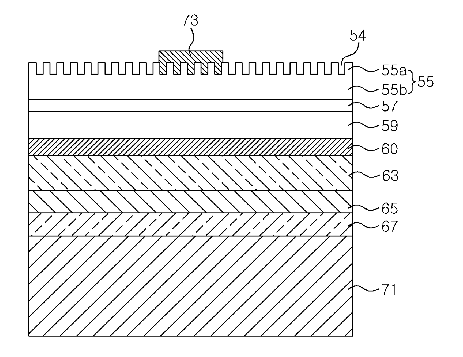
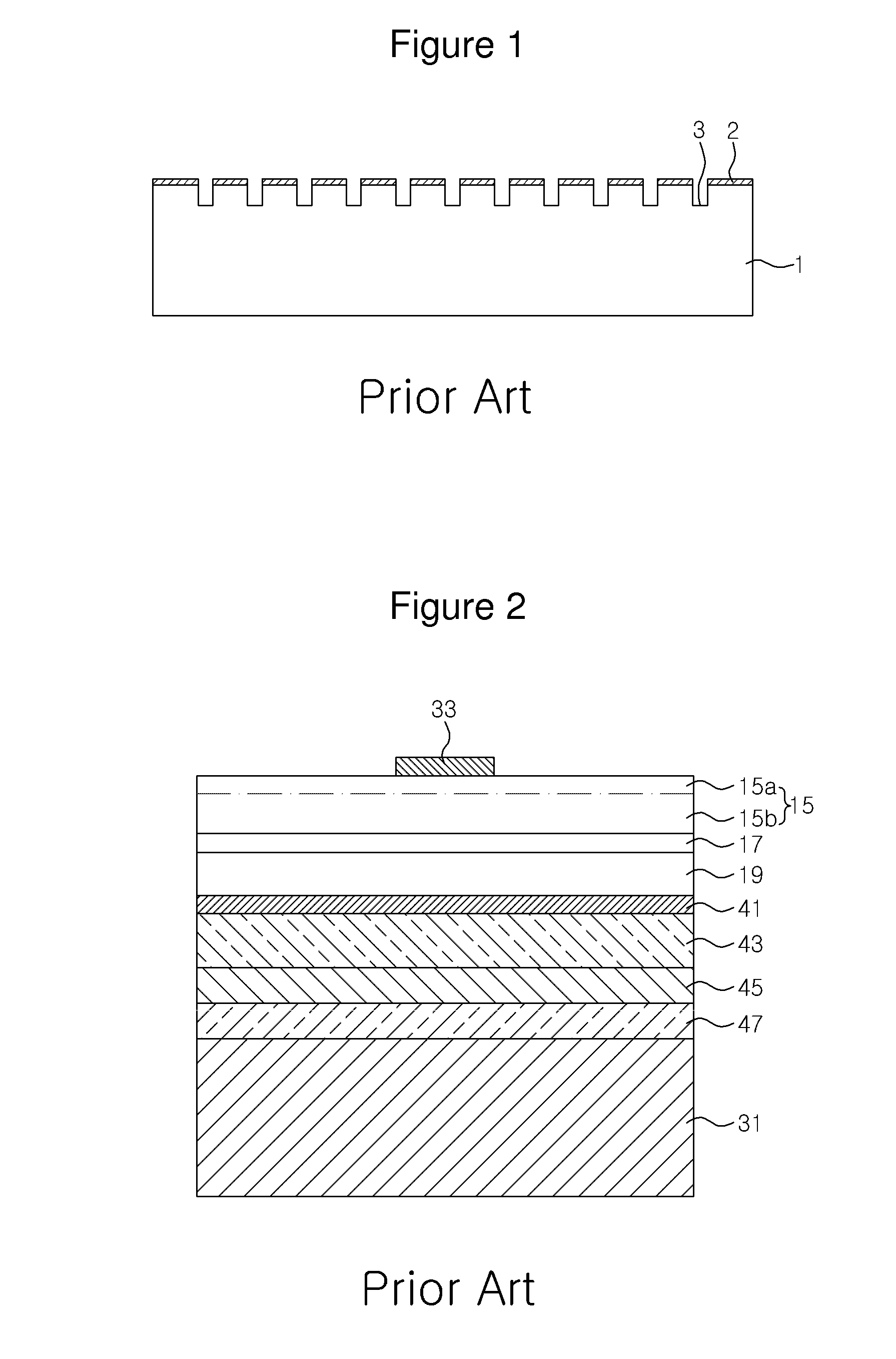
[0056]Hereinafter, preferred embodiments of the present invention will be described in detail with reference to the accompanying drawings. The following embodiments are provided only for illustrative purposes so that those skilled in the art can fully understand the spirit of the present invention. Therefore, the present invention is not limited to the following embodiments but may be implemented in other forms. In the drawings, the widths, lengths, thicknesses and the like of elements may be exaggerated for convenience of illustration. Like reference numerals indicate like elements throughout the specification.

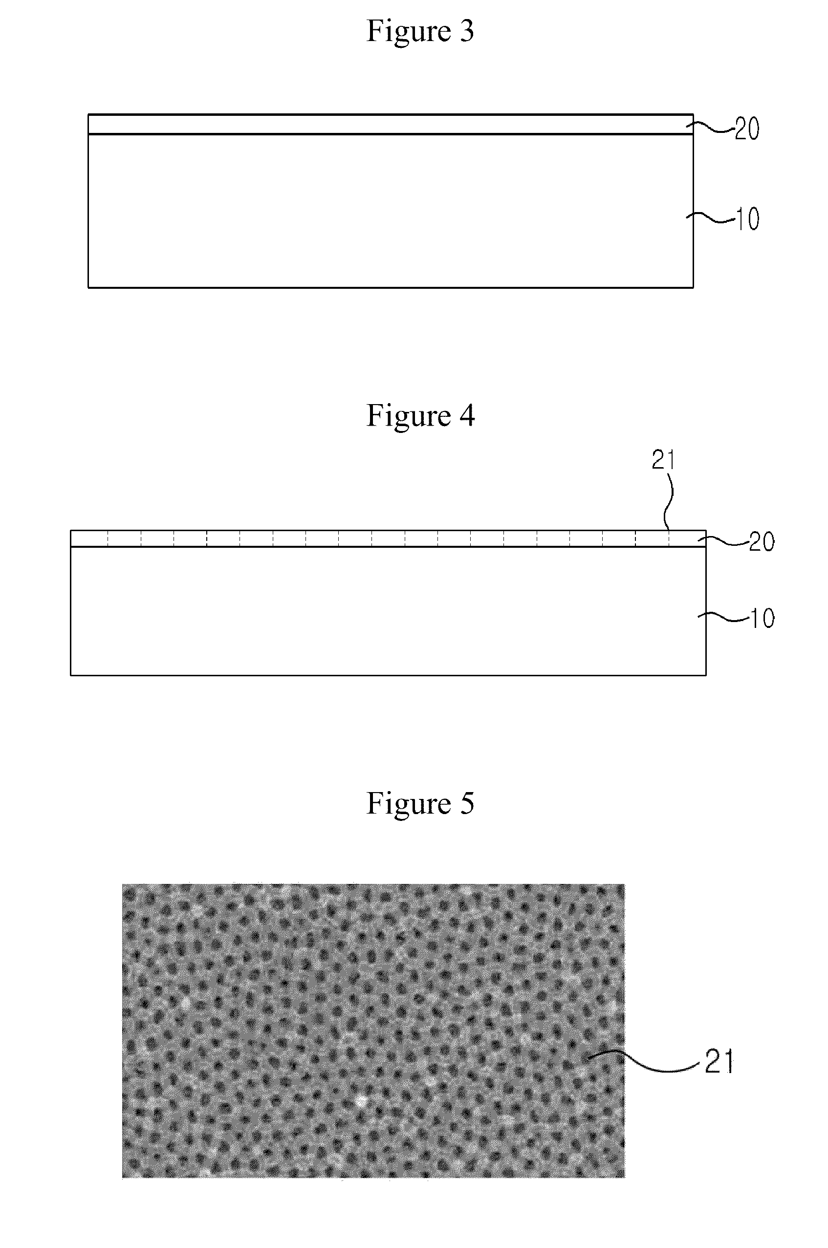
[0057]FIGS. 3 to 6 are views illustrating a process of fabricating a patterned substrate according to an embodiment of the present invention.

[0058]Referring to FIG. 3, an aluminum layer 20 is formed on a substrate 10. Here, a sapphire substrate may be used as the substrate 10.

[0059]The aluminum layer 20 is formed by depositing highly pure aluminum (99.999% Al) in a thickness ...


PUM

PropertyMeasurementUnit
widthaaaaaaaaaa
diameteraaaaaaaaaa
thicknessaaaaaaaaaa

Abstract

There is provided a method of fabricating a vertical light emitting diode. The method comprises the steps of: growing a low doped first conductive semiconductor layer on a sacrificial substrate; forming an aluminum layer on the low doped first conductive semiconductor layer; forming an AAO layer having a large number of holes formed therein by performing anodizing treatment of the aluminum layer; etching and patterning the low doped first conductive semiconductor layer using the aluminum layer with a large number of the holes as a shadow mask to expose a portion of the low doped first conductive semiconductor layer, thereby forming a large number of grooves; removing the aluminum layer remaining on the low doped first conductive semiconductor layer; sequentially forming a high doped first conductive semiconductor layer, an active layer and a second conductive semiconductor layer on the low doped first conductive semiconductor layer with a large number of the grooves; forming a metal reflective layer and a conductive substrate on the second conductive semiconductor layer; separating the sacrificial substrate; and forming an electrode pad on the other surface of the low doped first conductive semiconductor layer, the electrode pad being filled in a large number of the grooves to be in ohmic contact with the high doped first conductive semiconductor layer.

Description

CROSS-REFERENCE TO RELATED APPLICATIONS[0001]This application is the National Stage of International Application No. PCT / KR2007 / 006463, filed Dec. 12, 2007, and claims priority from and the benefit of Korean Patent Application No. 10-2006-0136681, filed on Dec. 28, 2006, Korean Patent Application No. 10-2006-0136682, filed on Dec. 28, 2006, and Korean Patent Application No. 10-2006-0136683, filed on Dec. 28, 2006, which are all hereby incorporated by reference for all purposes as if fully set forth herein.BACKGROUND OF THE INVENTION[0002]1. Field of the Invention[0003]The present invention relates to a light emitting device and a fabrication method thereof. More particularly, the present invention relates to a method of fabricating a substrate for a light emitting diode, on which patterns are formed using an anodic aluminum oxide (AAO) layer as a shadow mask; a vertical light emitting diode having a patterned semiconductor layer using an AAO layer and a fabrication method thereof, a...

Claims


Application Information

Patent Timeline
Patent Type & Authority Patents(United States)
IPC IPC(8): H01L27/15H01L33/00H01L33/22
CPCH01L33/0079H01L33/22H01L33/60H01L21/306H01L21/28H01L33/0093
Inventor YOON, YEO JINKIM, CHANG YEON
Owner SEOUL VIOSYS CO LTD
Why Eureka
Try Eureka