

Method for Manufacturing Semiconductor Device
- Summary
- Abstract
- Description
- Claims
- Application Information
AI Technical Summary
Benefits of technology
Problems solved by technology
Method used
Image

Examples
embodiment mode 1
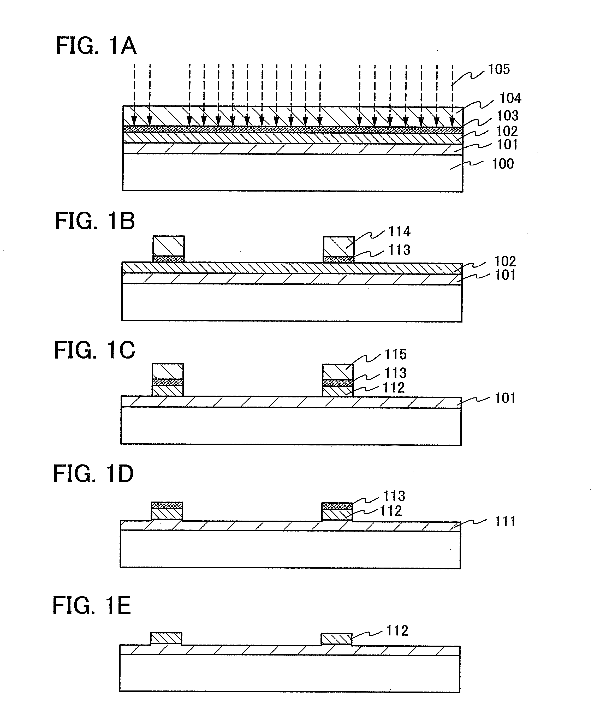
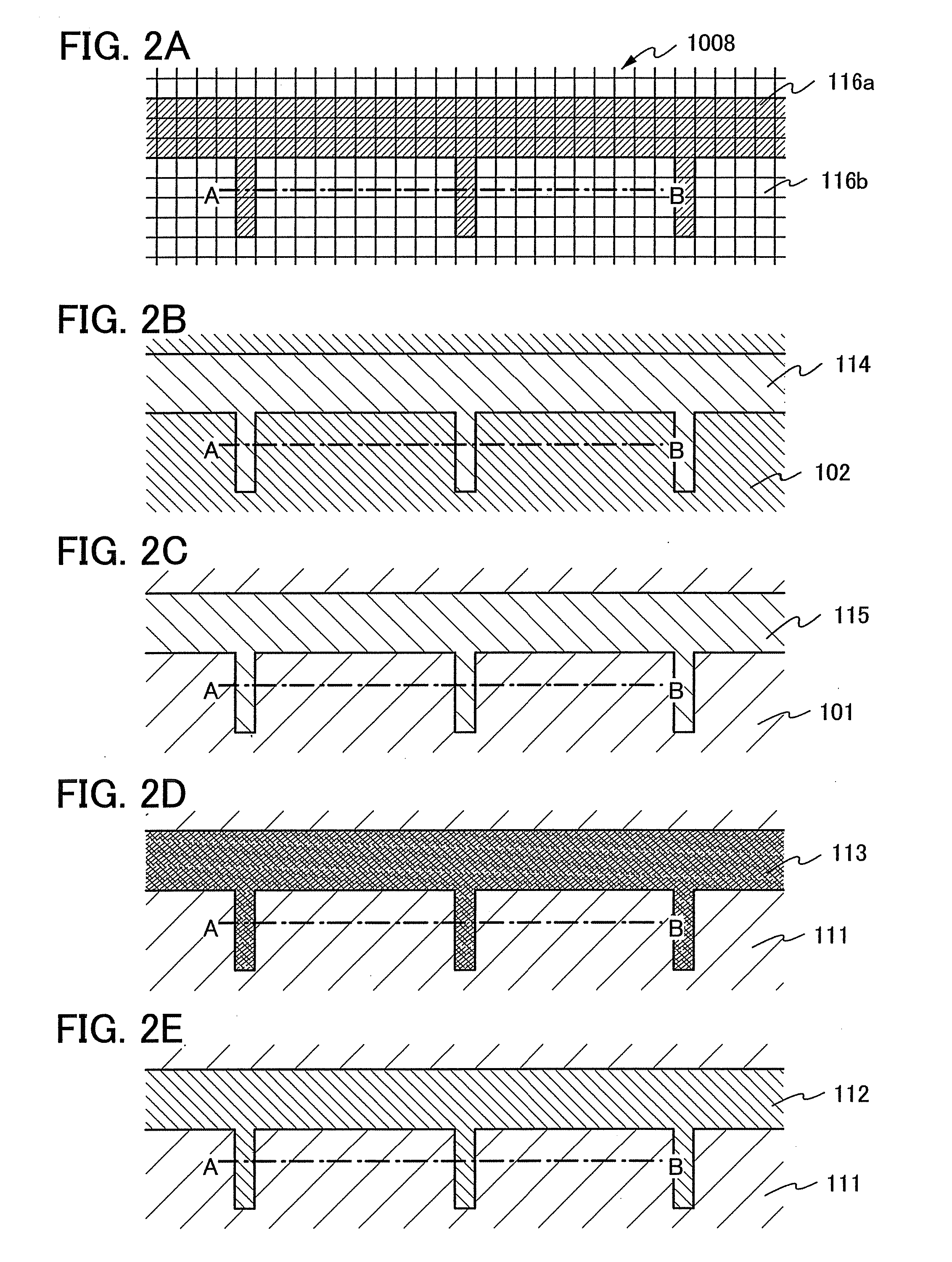
[0061]In this embodiment mode, a laser ablation patterning process (LAPP) in which a thin film is processed using a laser beam without using a photolithography process will be described. FIGS. 1A to 1E, FIGS. 3A to 3E, and FIGS. 5A to 5E are cross-sections showing a process in which a layer with a desired shape is selectively formed over a substrate. FIGS. 2A to 2E, FIGS. 4A to 4E, and FIGS. 6A to 6E show electrooptic elements of a laser irradiation apparatus and top views of FIGS. 1A to 1E, FIGS. 3A to 3E, and FIGS. 5A to 5E. This embodiment mode will be described with reference to a mode in which a wiring is formed.
[0062]As shown in FIG. 1A, a first layer 101 which serves as a base film is formed over one side of a substrate 100, a second layer 102 is formed over the first layer 101, a light absorbing layer 103 is formed over the second layer 102, and a layer 104 having a light-transmitting property is formed over the light absorbing layer 103.
[0063]As the substrate 100, a glass s...
embodiment mode 3
[0121]In this embodiment mode, a process for forming a layer having a desired shape which differs to that in Embodiment Mode 1 will be described with reference to FIGS. 5A to 5E and FIGS. 6A to 6E. In this embodiment mode, the process for removing a light absorbing layer differs to those in Embodiment Modes 1 and 2.
[0122]As shown in FIG. 5A, similarly to in Embodiment Mode 1, the first layer 101 is formed over the substrate 100, the second layer 102 is formed over the first layer 101, the light absorbing layer 103 is formed over the second layer 102, and the layer 104 having a light-transmitting property is formed over the light absorbing layer 103.
[0123]In this embodiment mode, preferably the etching rate of the light absorbing layer 103 and the second layer 102 differs substantially to that of the layer 104 having a light-transmitting property. Representatively, preferably the etching rate of the light absorbing layer 103 and the second layer 102 is faster than that of the layer 1...
embodiment mode 4
[0132]In this embodiment mode, an etching process which can be applied to any of Embodiment Modes 1 to 3 will be described with reference to FIGS. 8A to 8E. Note that although description is made with reference to Embodiment Mode 1 here, this process can be applied to Embodiment Modes 2 and 3, as appropriate.
[0133]As shown in FIG. 8A, similarly to in Embodiment Mode 1, the first layer 101 is formed over the substrate 100, the second layer 102 is formed over the first layer 101, the light absorbing layer 103 is formed over the second layer 102, and the layer 104 having a light-transmitting property is formed over the light absorbing layer 103.
[0134]Next, the light absorbing layer 103 is irradiated with the laser beam 105 through the layer 104 having a light-transmitting property.
[0135]As a result, as shown in FIG. 8B, a part of the layer having a light-transmitting property and a part of the light absorbing layer which have been irradiated with the laser beam 105 are removed, and the...
PUM
 Abstract
Description
Claims
Application Information