Semiconductor package structure and fabrication method thereof

Active Publication Date: 2018-08-23
SAMSUNG ELECTRONICS CO LTD
View PDF7 Cites 14 Cited by
  • Summary
  • Abstract
  • Description
  • Claims
  • Application Information

AI Technical Summary

Benefits of technology

[0034]According to an exemplary embodiment, a semiconductor package structure includes: a base substrate; a die disposed on the base substrate to include a semiconductor device; a solder bump disposed on a surface of the die, and configured to dissipate heat generated in the die to an outside, and a solder ball disposed on another surface, opposite to the surface, of the die to transmit a signal produced by the semiconductor device of the die to an external device. Thus, by a reflow process of the solder bump, the die may be self-aligned to the base substrate. Accordingly, a process margin may be improved, and thus, a fabrication yield may be improved. In addition, a fabrication process may be simplified to provide a semiconductor package s

Problems solved by technology

Furthermore, in terms of performance of a device and efficiency in characteristics of the device, heat generated in an application processor affects performance of a device and causes reduction in a life span of the device and deterioration in reliability, and thus, efficiently removing heat generated in a process of operating the device is also considered as an emerging issue.
In addition,

Method used


Image

  • Semiconductor package structure and fabrication method thereof
  • Semiconductor package structure and fabrication method thereof
  • Semiconductor package structure and fabrication method thereof

Examples


first embodiment

[0085]According to modified examples of the first exemplary embodiment, the first solder bump 122 may be provided on the die 200, and then, may be bonded to the heat dissipation plug 112 of the base substrate 100, unlike that described with reference to FIGS. 1 to 8. Hereinafter, a method of fabricating a semiconductor package structure, according to the modified examples of the present invention, will be described with reference to FIGS. 10 and 11.

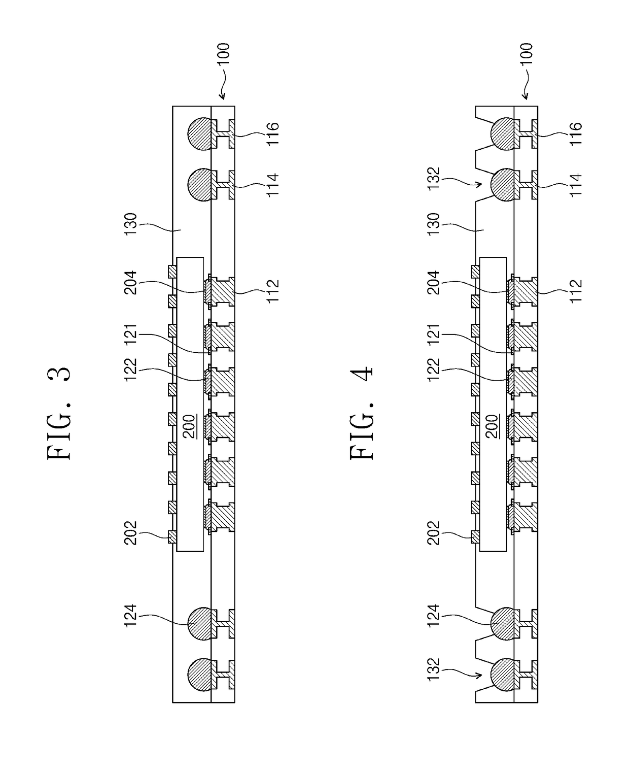
[0086]FIG. 10 is a diagram illustrating a method of fabricating a semiconductor package structure, according to a first modified example of the first exemplary embodiment.

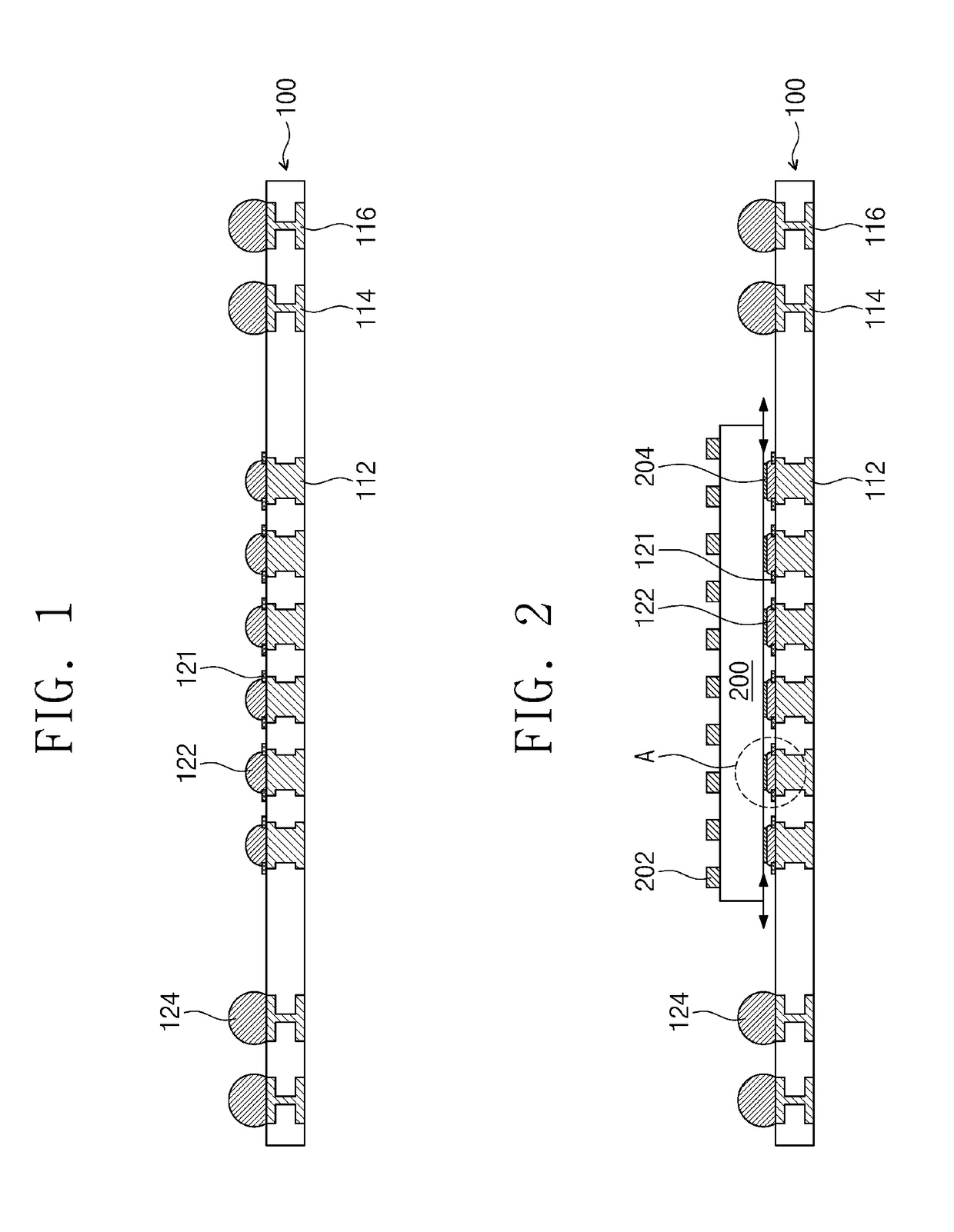
[0087]Referring to FIG. 10, the die 200 described with reference to FIG. 2 and the base substrate 100 described with reference to FIG. 1 are prepared. The first solder bump 122 described with reference to FIG. 1 may be provided on the joining pattern 204 of the die 200.

[0088]The first solder bump 122 may be formed on the joining pattern 204 of the die 200, and then, the ...

second embodiment

[0132]According to a modified example of the second embodiment, a semiconductor package structure may be provided to have a package-on-package (POP) structure, unlike the afore-described second exemplary embodiment. Hereinafter, a semiconductor package structure according to the modified example of the second exemplary embodiment will be described with reference to FIG. 19.

[0133]FIG. 19 is a diagram illustrating a semiconductor package structure according to the modified example of the second exemplary embodiment.

[0134]Referring to FIG. 19, a first semiconductor package structure P2a and a second semiconductor package structure P2b, according to the second exemplary embodiment described with reference to FIG. 18, may be provided. The second semiconductor package structure P2b may be disposed on the first semiconductor package structure P2a.

[0135]The first semiconductor package structure P2a and the second semiconductor package structure P2b may be electrically connected to each oth...


PUM


Abstract

A method of fabricating a semiconductor package structure is provided. The structure is configured to include a base substrate, a die disposed on the base substrate, the die including a semiconductor device, a solder bump disposed on a surface of the die, and configured to discharge heat generated in the die to an outside; and a solder ball disposed on another surface, opposite to the surface, of the die, and configured to transmit a signal, which is produced by the semiconductor device of the die, to an external device.

Description

TECHNICAL FIELD[0001]The inventive concept relates to a semiconductor package structure and a fabrication method thereof. If, in the case of using a metal layer formed on a back side of a flip chip die and a solder formed thereon in a wafer- or panel-level fan-out electronic packaging, the die placed on a substrate is reflowed, the die and a metal pad on the substrate are automatically self-aligned to each other, when temperature of the melted solder is returned to a room temperature, thereby allowing the die to be formed on the substrate with a high positional accuracy. In the exemplary embodiments of the inventive concept, this phenomenon is used to fabricate a package of a semiconductor device requiring many input / output terminals. In addition, it relates to a semiconductor package structure including a heat dissipation plug, which discharges heat generated in the die to the outside, and a fabrication method thereof.BACKGROUND ART[0002]An application processor, which is one of ke...

Claims


Application Information

Patent Timeline
IPC IPC(8): H01L23/367H01L23/373H01L23/40H01L23/492H01L23/00
CPCH01L23/367H01L23/3738H01L23/40H01L23/492H01L24/19H01L2224/04105H01L2224/12105H01L2224/73259H01L2924/15153H01L23/3677H01L23/3736H01L23/49816H01L23/5389H01L25/105H01L2224/81192H01L2224/92224H01L2224/13111H01L2224/13116H01L2224/13144H01L2224/24227H01L2224/81191H01L2224/16235H01L2224/16227H01L2224/81815H01L2224/0401H01L2924/15313H01L24/92H01L24/13H01L24/81H01L2224/16106H01L2924/18162H01L24/16H01L2225/1023H01L2225/1094H01L2225/1058H01L25/0655H01L2924/00014H01L23/3735H01L23/481H01L23/488H01L2224/16225H01L2224/19
Inventor KIM, YOUNGHOPARK, HWANPIL
Owner SAMSUNG ELECTRONICS CO LTD
Why Eureka
Try Eureka