
Eureka
For R&D, Eureka makes reading and utilizing patents & technical documents easy.
Eureka AIR
Designed for self-driven R&D workflows. Generate viable solutions, solve complex R&D challenges, empower your innovation with AI.

Eureka Materials
Designed for material experts only. Revolutionize your material R&D, from search, analyze, to developing new materials.

TechResearch
Generate reliable direction feasibility study reports for your R&D in just a few steps.

TechSeek
Discover and master advanced knowledge NOW. Basics, ideas, possibilities, all at once.

TechMind
As an expert in R&D Theories, TechMind can generates customized viable solutions instantly.

TechRisk
Analyze your overall solution with one click, know your potential R&D risks in advance.

TechMonitor
Get weekly tech updates, stay abreast of the latest tech innovations and key insights.
Semiconductor device and display device having the same
- Summary
- Abstract
- Description
- Claims
- Application Information
AI Technical Summary
Benefits of technology
Problems solved by technology
Method used
Image

Examples
embodiment 1
[0069]In this embodiment, a semiconductor device of one embodiment of the present invention will be described with reference to FIGS. 1A to 1C, FIGS. 2A to 2C, FIGS. 3A and 3B, FIGS. 4A to 4C, FIGS. 5A and 5B, FIGS. 6A to 6C, FIGS. 7A to 7D, FIGS. 8A to 8D, FIGS. 9A and 9B, FIGS. 10A to 10D, FIGS. 11A to 11C, FIGS. 12A and 12B, FIGS. 13A to 13D, FIGS. 14A and 14B, FIGS. 15A to 15D, FIGS. 16A to 16D, FIGS. 17A to 17F, FIGS. 18A to 18F, and FIGS. 19A to 19F.
Structure Example 1 of Semiconductor Device
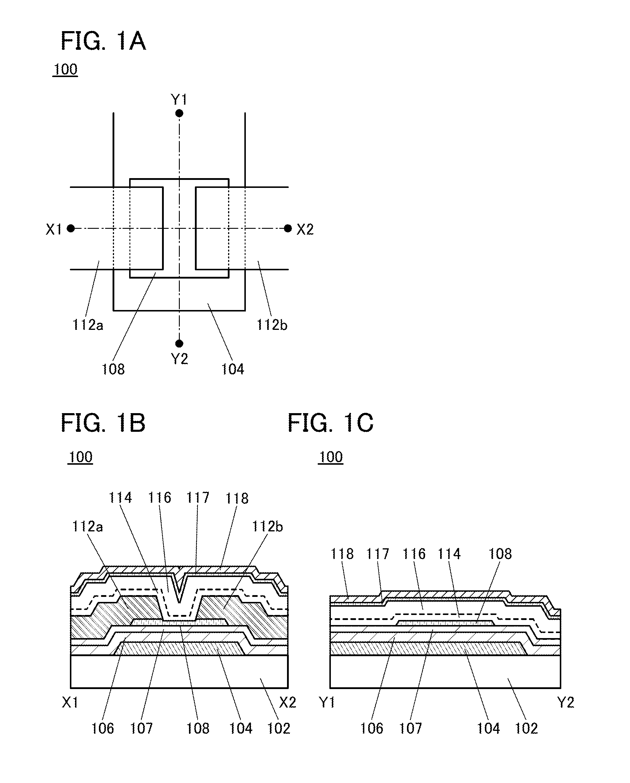
[0070]FIG. 1A is a top view of a transistor 100 that is a semiconductor device of one embodiment of the present invention. FIG. 1B is a cross-sectional view taken along a dashed dotted line X1-X2 in FIG. 1A, and FIG. 1C is a cross-sectional view taken along a dashed dotted line Y1-Y2 in FIG. 1A. Note that in FIG. 1A, some components of the transistor 100 (e.g., an insulating film serving as a gate insulating film) are not illustrated to avoid complexity. Furthermore, the direction of the d...
example 6
Structure Example 6 of Semiconductor Device
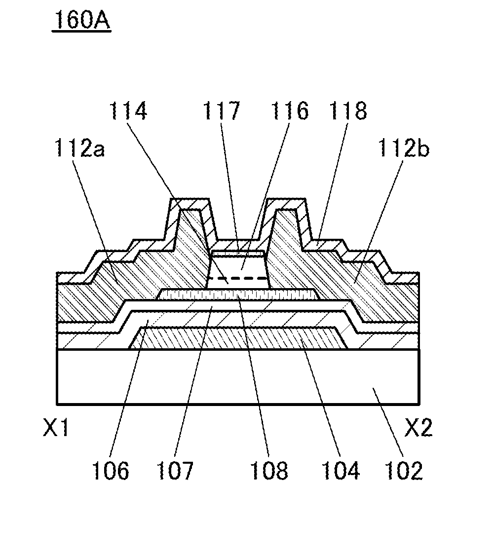
[0154]A structure example different from that of the transistor 100 in FIGS. 1A to 1C is described with reference to FIGS. 6A to 6C. Note that in the case where a portion has a function similar to that described above, the same hatch pattern is applied to the portion, and the portion is not especially denoted by a reference numeral in some cases.
[0155]FIG. 6A is a top view of a transistor 170 that is a semiconductor device of one embodiment of the present invention. FIG. 6B is a cross-sectional view taken along a dashed dotted line X1-X2 in FIG. 6A, and FIG. 6C is a cross-sectional view taken along a dashed dotted line Y1-Y2 in FIG. 6A.
[0156]The transistor 170 includes the conductive film 104 functioning as a gate electrode over the substrate 102, the insulating film 106 over the substrate 102 and the conductive film 104, the insulating film 107 over the insulating film 106, the oxide semiconductor film 108 over the insulating film 107, the...
example 7
Structure Example 7 of Semiconductor Device
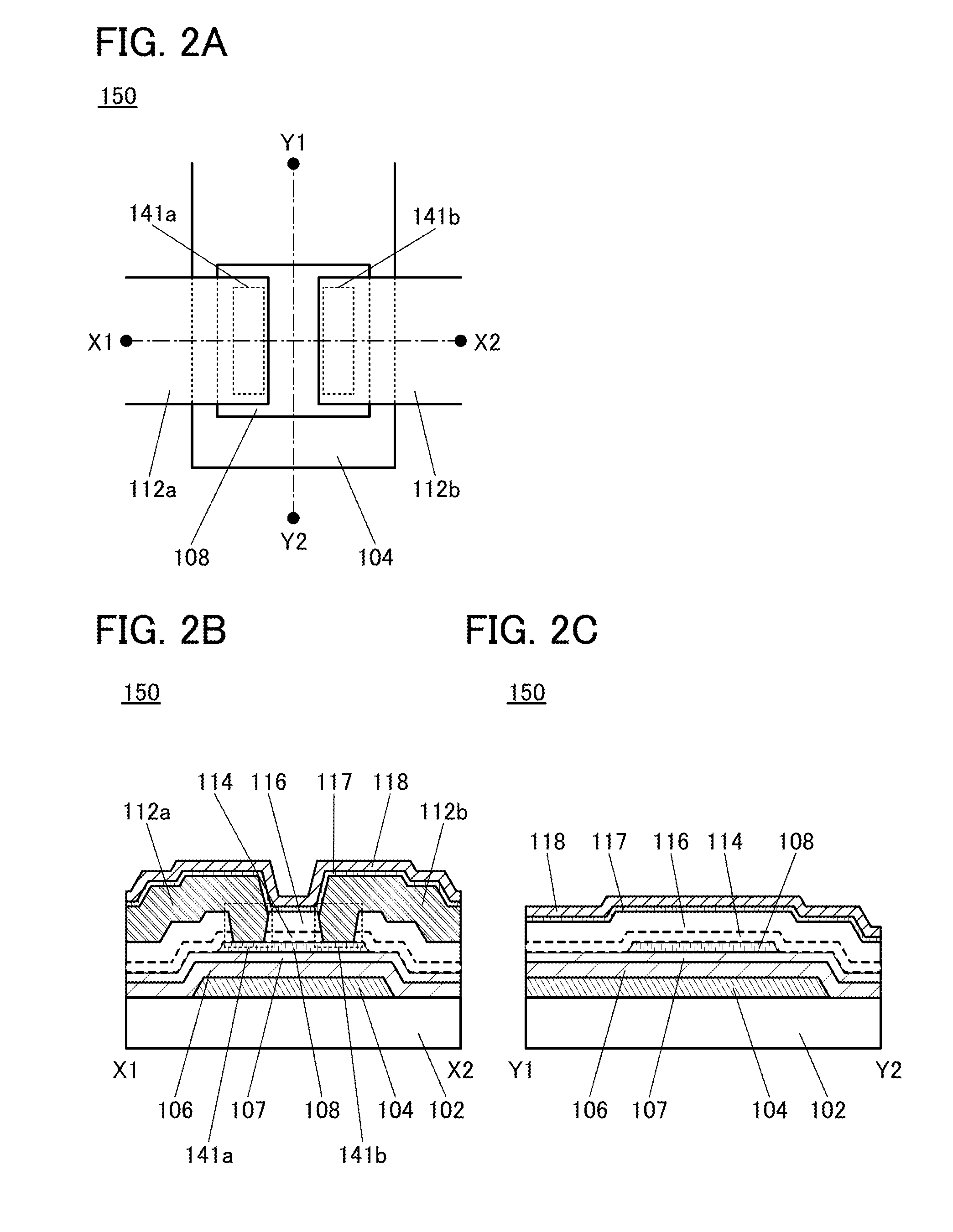
[0165]Structure examples different from that of the transistor 170 in FIGS. 6A to 6C are described with reference to FIGS. 7A to 7D. Note that in the case where a portion has a function similar to that described above, the same hatch pattern is applied to the portion, and the portion is not especially denoted by a reference numeral in some cases.
[0166]FIG. 7A is a cross-sectional view in the channel length direction of a transistor 170A, and FIG. 7B is a cross-sectional view in the channel width direction of the transistor 170A. FIG. 7C is a cross-sectional view in the channel length direction of a transistor 170B, and FIG. 7D is a cross-sectional view in the channel width direction of the transistor 170B. Note that top views of the transistor 170A and the transistor 170B are omitted here because they are similar to the top view of FIG. 6A. Note that in the case where a portion has a function similar to that described above, the same hatch ...
PUM
 Abstract
Description
Claims
Application Information
 - R&D Engineer
- R&D Manager
- IP Professional
- Industry Leading Data Capabilities
- Powerful AI technology
- Patent DNA Extraction
Browse by: Latest US Patents, China's latest patents, Technical Efficacy Thesaurus, Application Domain, Technology Topic, Popular Technical Reports.
© 2024 PatSnap. All rights reserved.Legal|Privacy policy|Modern Slavery Act Transparency Statement|Sitemap|About US| Contact US: help@patsnap.com