Retardation film and fabrication method thereof
a technology of retardation film and fabrication method, which is applied in the direction of polarising elements, paper/cardboard containers, instruments, etc., can solve the problems of increasing the cost of fabricating the photomask, reducing yield, and poor quality of the retardation film, so as to achieve the effect of massive production of high-quality retardation film and avoiding product defects
- Summary
- Abstract
- Description
- Claims
- Application Information
AI Technical Summary
Benefits of technology
Problems solved by technology
Method used
Image
Examples
embodiment a1
[0066] irradiating the photo-orientable layer with the first linearly-polarized ultraviolet light before irradiating the photo-orientable layer with the second linearly-polarized ultraviolet light, and the width of the opacifier stripes is 50 μm.
[0067]Method of preparating the retardation film in embodiment A1 includes following steps:
[0068](1-1) Preparation of the Opacifier Pattern.
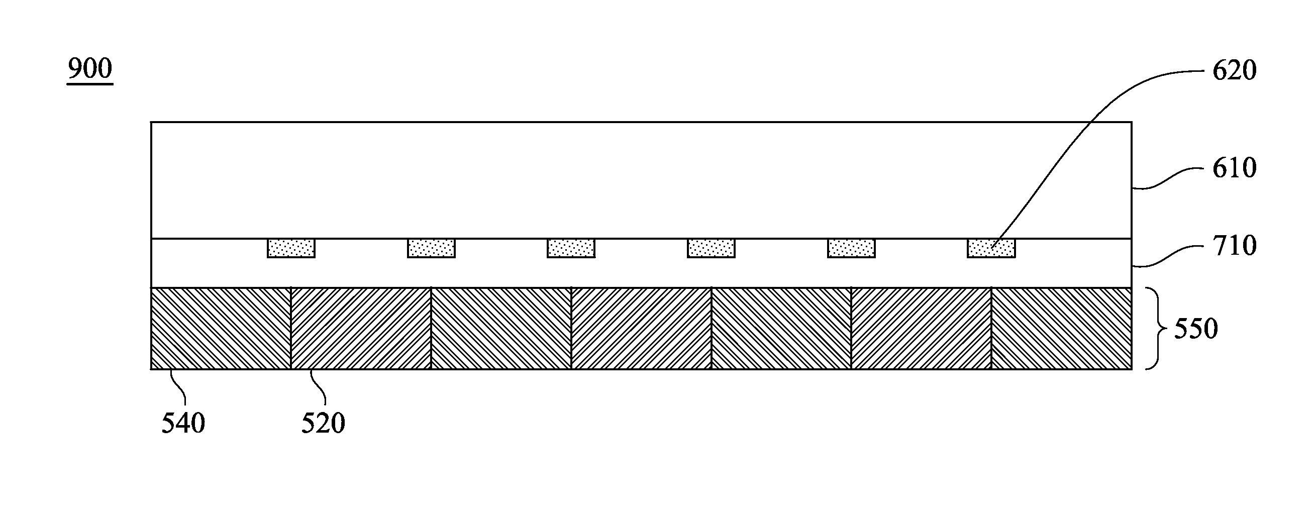
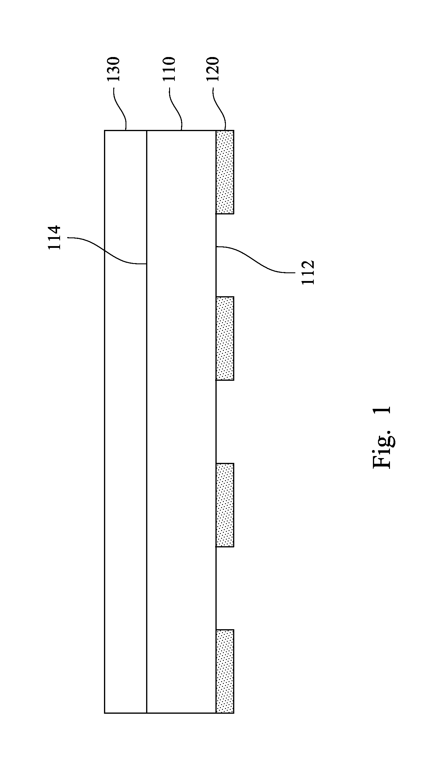
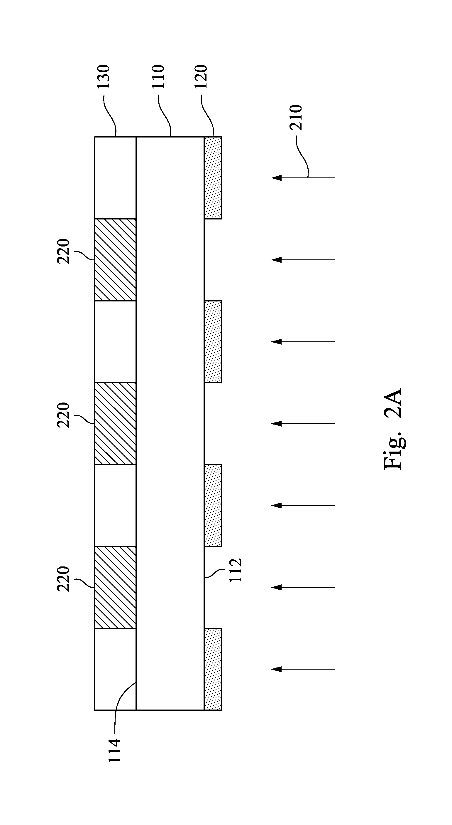
[0069]The light-shielding solution is gravure printed on a first surface of a polycarbonate substrate (a primary transparent substrate, having a thickness of 60 μm, a birefringence of 2.17×10⁻⁴ and a retardation of 13 nm) according to a predetermined pattern, and a printed thickness is about 1 μm. Then, the polycarbonate substrate and the light-shielding solution are baked in an oven under 60° C. for 30 seconds. Therefore, a substrate having the opacifier pattern thereon is formed, and a light transmissibility of the substrate covered by the opacifier pattern is 10%.
[0070](1-2) Preparation of the Photo-O...
embodiment
[0087 A2 is similar to embodiment A1, the difference between the two embodiments is by changing the width of the opacifier stripes to 100 μm in step (1-7).
[0088]Embodiment A3: irradiating the photo-orientable layer with the second linearly-polarized ultraviolet light before irradiating the photo-orientable layer with the first linearly-polarized ultraviolet light, and the width of the opacifier stripes is 50 μm.
[0089]Embodiment A3 is similar to embodiment A1, the difference between the two embodiments is by changing step (1-3) and step (1-4). As described below:
[0090](1-3) First Irradiating.
[0091]Irradiating the photo-orientable layer prepared in step (1-2) with a second linearly-polarized ultraviolet light in a direction from the second surface toward the first surface of the primary transparent substrate (irradiation dosage of the second linearly-polarized ultraviolet light is 90 mJ / cm2, as shown in FIG. 3A), which the slow axis of the primary transparent substrate forms an angle ...
PUM
| Property | Measurement | Unit |
|---|---|---|
| width | aaaaa | aaaaa |
| width | aaaaa | aaaaa |
| thickness | aaaaa | aaaaa |
Abstract
Description
Claims
Application Information


