Smart Card Module

a card module and card chip technology, applied in the field of smart card modules, can solve the problems of increasing manufacturing time and costs, complex electrical connection between the antenna and the chip, and failure of the connection, so as to improve the strength of the electromagnetic connection, increase the antenna length, and increase the thickness of the antenna

Inactive Publication Date: 2015-11-12
JOHNSON ELECTRIC SA
View PDF7 Cites 23 Cited by
  • Summary
  • Abstract
  • Description
  • Claims
  • Application Information

AI Technical Summary

Benefits of technology

[0020]Furthermore, the antenna may extend from one said side of the circuit substrate to the other said side of the circuit substrate through a via hole in the circuit substrate. This increases the length of the antenna, which in turn improves the strength of the electromagnetic connection between the antenna of the smart card module and the antenna on the smart card reader. Even more preferably, the portion of the antenna on the first said side is identically sized and shaped to the portion of the antenna on the second said side, such that the two portions are substantially superposed on the circuit substrate.
[0021]The circuit substrate may be folded such that the antenna overlaps onto itself, increasing the thickness of the antenna. This further improves a strength of the electromagnetic connection between the antenna of the smart card module and the antenna on the smart card reader.

Problems solved by technology

It is complex to establish electrical connection between the antenna and the chip, and it is known for such connection to fail when manufacturing smart cards.
This increases manufacturing time and costs.
Providing the antenna in the smart card also produces non-planarity across the surface of the smart card, such that the card may not be perfectly even.
This is not aesthetically pleasing.
However, providing a secondary antenna on the smart card does not solve the non-planar aesthetic issue.
Furthermore, the process of providing a secondary antenna on the smart card is expensive and requires certain material to be used so that the antenna can be embossed to the smart card.
The manufacturing process is more complicated than the single antenna production process, thus adding to time and costs.
Furthermore, connection between the two antennae cannot be tested until the smart card module has been assembled with the body of the smart card.
Thus defective cards cause greater waste.
However, the proximity between the smart card module antenna and the metallic contact pad means that the contact pad interferes with the electromagnetic connection between the smart card module antenna and the card reader antenna.
Furthermore, as the size of the antenna is limited by the size of the module, the performance of such antenna is not satisfactory.
This may deform the contact pad and break the connection between the contact pad and the chip, rendering the smart card defective.

Method used


Image

  • Smart Card Module
  • Smart Card Module
  • Smart Card Module

Examples


first embodiment

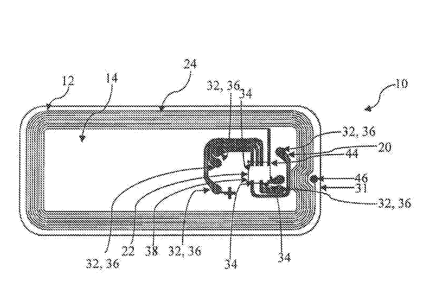
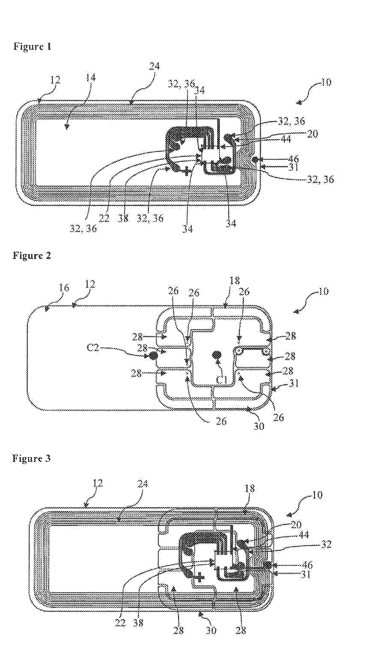
[0044]Referring firstly to FIGS. 1 to 4, there is shown an embedded smart card module 10 forming part of a dual-interface smart card, such as a bank card, identification card, health card, SIM card or any other similar dual-interface device. The smart card module 10 comprises an extended or elongated circuit substrate 12 having a first side or surface 14 and an opposing second side or surface 16, which are preferably planar. A card-reader contact element 18 is mounted to the second side 16 of the circuit substrate 12.

[0045]An integrated circuit contact element 20 is in electrical communication with the card-reader contact element 18, through the circuit substrate 12. The integrated circuit contact element 20 defines a connection area at one end for mounting to the first side 14 of the circuit substrate 12 an integrated circuit, in the form of a chip 22. At the other end, the integrated circuit contact element 20 passes through via holes 26 to connect with the card-reader contact ele...

second embodiment

[0073]The second embodiment has the added advantage of offsetting the chip 22 from the card-reader contact element 18, so that in the event the card-reader contact element 18 is deformed by impact during insertion of the smart card 110 into the card reader, the connection between the card-reader contact element 18 and the chip 22 remains unaffected.

[0074]Shown in FIGS. 7 to 10 is the third embodiment of the smart card module 210. This embodiment is substantially identical to that of the first embodiment, except that the antenna coil 224 does not extend around the whole circumferential perimeter of the elongated circuit substrate 12. Instead, the antenna coil 224 is provided entirely offset from the card-reader contact element 18.

[0075]Each turn of the antenna coil 224 in this embodiment is therefore not as long as each turn of the antenna coil 24 of the first or second embodiments. However, as the whole of the antenna coil 224 is offset from the card-reader contact element 18, inter...

sixth embodiment

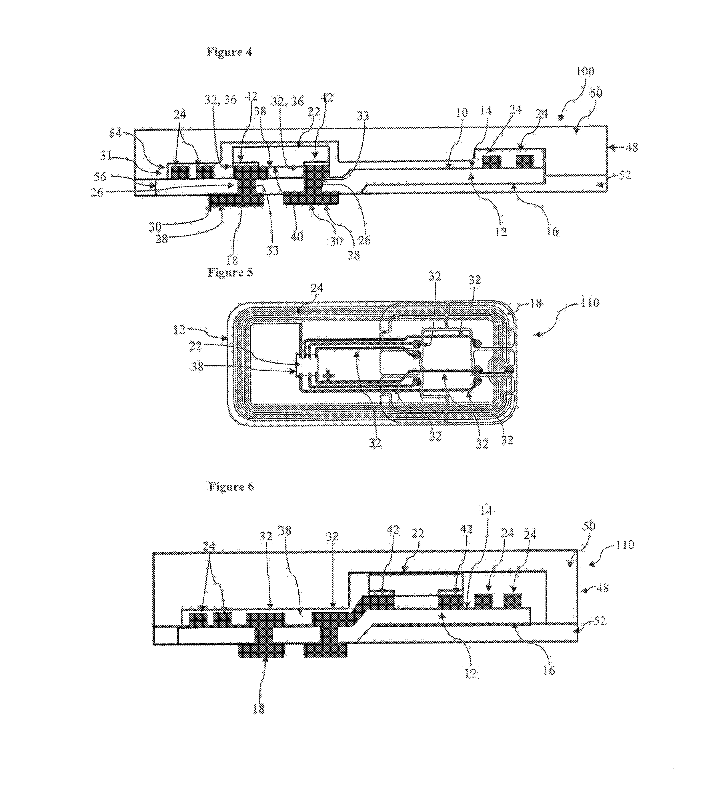
[0080]Alternatively, a capacitor 560 may be provided integrally with the circuit substrate 12, as shown in the smart card module 510 in FIG. 13. Such a substrate capacitor 560 may function identically to the separate component capacitor 60, shown in FIG. 12, and advantageously boosts the performance of the antenna coil 24.

[0081]In this embodiment, the substrate capacitor 560 is provided offset from the card-reader contact element 18 and integrated circuit 22, and is connected in parallel to the antenna 24 and chip 22 via a circuit contact member 32.

[0082]It will be appreciated that the capacitor 60, 560 may be positioned in a variety of positions about the substrate 12, the embodiments shown in FIGS. 12 and 13 being just two examples thereof. The capacitor 60, 560 may be positioned on either side 14, 16 of the substrate 12, adjacent to the card-reader contact element 18, or offset from the card-reader contact element 18.

[0083]Alternatively or additionally, one or more said capacitor...


PUM


Abstract

A smart card module has an elongated circuit substrate; a card-reader contact element on one side of the substrate for connection to a smart card reader; an integrated circuit connection element on another side of the substrate connected to the card-reader contact element and to which an integrated circuit is mountable; and an antenna on the substrate connected to the integrated circuit connection element for receiving radio frequency signals from the smart card reader. A furthest perimeter edge of the antenna is spaced from a proximal edge of the card-reader contact element by at least half a distance between the proximal edge and a center C1 of the card-reader contact element. Thus a larger antenna coil can be accommodated on the substrate with less overlap of the card-reader contact element, whilst also enabling a separate module to be integrated with the smart card.

Description

CROSS REFERENCE TO RELATED APPLICATIONS[0001]This non-provisional patent application claims priority under 35 U.S.C. §119(a) from Patent Application No. 1407977.6 filed in The United Kingdom on May 6, 2014, the entire contents of which are hereby incorporated by reference.FIELD OF THE INVENTION[0002]The present invention relates to a smart card module, a smart card having such a smart card module, such as a bank card or SIM card, a method of forming such a smart card module, and to a method of forming a smart card having such a smart card module.BACKGROUND OF THE INVENTION[0003]Smart card modules are well known and are used in smart cards, also known as chip cards or integrated circuit cards. Such smart cards are typically dual interface smart cards, whereby they can communicate with a card reader with and without direct contact.[0004]A smart card module usually comprises a contact pad on one side of a module substrate and a chip mounted on the other side of the substrate. The chip ...

Claims


Application Information

Patent Timeline
Patent Type & Authority Applications(United States)
IPC IPC(8): G06K19/08G06K19/077
CPCG06K19/08G06K19/07783G06K19/07754G06K19/07743G06Q20/341G06K19/07769G06K19/07749G06K19/044G06K19/045
Inventor LINFIELD, CALVIN JOHN
Owner JOHNSON ELECTRIC SA
Why Eureka
Try Eureka