Reticle Inspection Using Near-Field Recovery

Active Publication Date: 2015-11-12
KLA TENCOR CORP
View PDF9 Cites 21 Cited by
  • Summary
  • Abstract
  • Description
  • Claims
  • Application Information

AI Technical Summary

Benefits of technology

The patent describes a computer-implemented method for detecting defects on a reticle, which is a critical component in the manufacturing process of semiconductor devices. The method involves separating pattern information on the reticle into predetermined segments, determining near-field data for the segments, and generating a data structure that includes pairs of segments and the near-field data. During the inspection process, the method assigns the near-field data to the segments based on their similarity to the inspection area. The method can be performed using computer systems and has been found to be effective in detecting defects on reticles.

Problems solved by technology

However, there is no practical method of solving Maxwell's equations accurately for an entire reticle in the required inspection time, which is one to two hours.
However, this limits the accuracy of the calculated image and therefore limits the smallest defect that can be detected.
Advancement in optical proximity correction (OPC) results in ever-increasing complexity in the patterns written on a photomask or reticle.
It becomes more and more difficult to separate critical (printing) defects from non-critical (nuisance) defects due to the OPC complexity.
There are, however, a number of disadvantages of such currently used methods and systems.
Increased OPC complexity means oftentimes the user has difficulty separating the printing defects from non-printing defects with a few empirical rules.
In addition, potentially large numbers of defects can overload the user and prevent finishing the defect disposition in a reasonable time period.
Increased OPC complexity with inverse lithography technology (ILT) can limit the usefulness of the method.
However, the accuracy of such tools is never fully independently verified.
More critically, such methods do not consider the complex photoresist development or etching process after imaging is done on a scanner.
Studies have shown that there is a poor correlation between the defect size measured on an aerial imaging tool and that measured on a wafer.

Method used


Image

  • Reticle Inspection Using Near-Field Recovery
  • Reticle Inspection Using Near-Field Recovery
  • Reticle Inspection Using Near-Field Recovery

Examples


Embodiment Construction

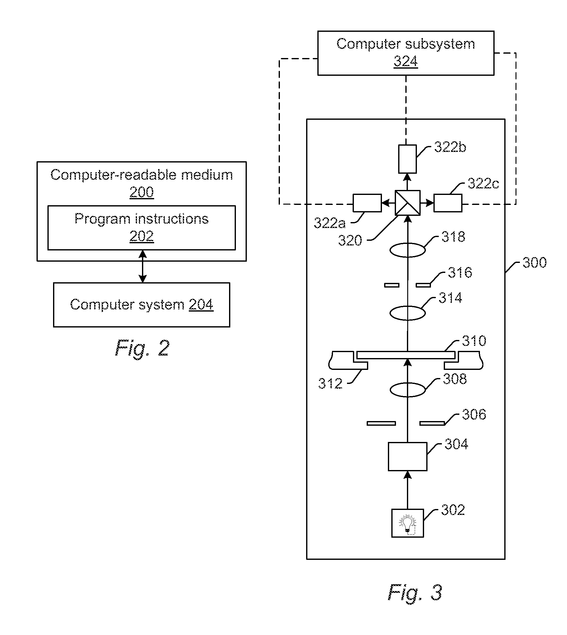
[0027]Turning now to the drawings, it is noted that the figures are not drawn to scale. In particular, the scale of some of the elements of the figures is greatly exaggerated to emphasize characteristics of the elements. It is also noted that the figures are not drawn to the same scale. Elements shown in more than one figure that may be similarly configured have been indicated using the same reference numerals. Unless otherwise noted herein, any of the elements described and shown may include any suitable commercially available elements.

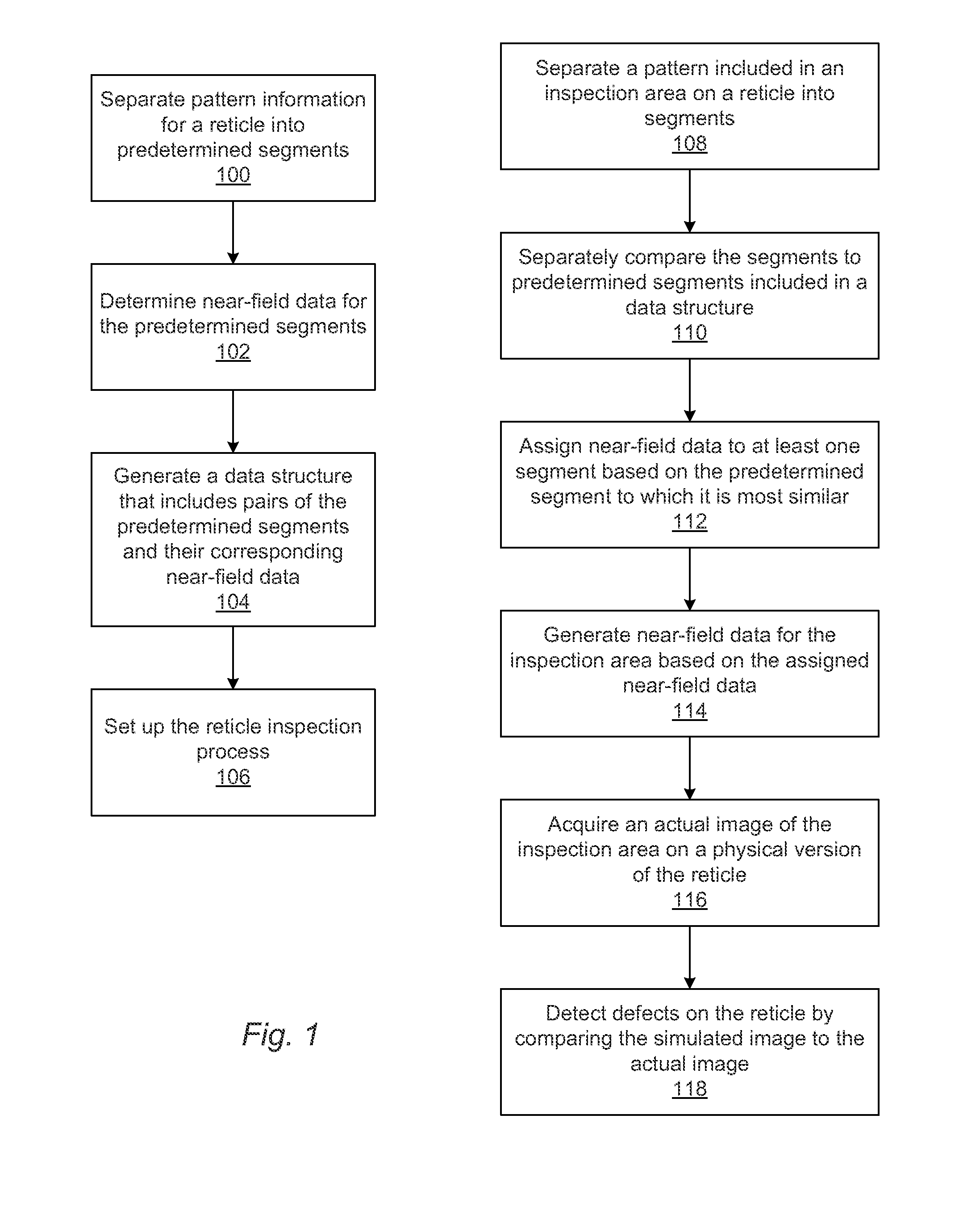
[0028]The embodiments described herein generally relate to inspecting reticles by making use of a database that describes the reticle pattern. For example, as described further herein, the embodiments may be used for die-to-database inspection of reticles using near-field recovery. The embodiments described herein may be used for inspecting reticles for pattern defects and contamination.

[0029]The terms “reticle,”“mask,” and “photomask” are used inter...


PUM


Abstract

Systems and methods for detecting defects on a reticle are provided. The embodiments include generating and / or using a data structure that includes pairs of predetermined segments of a reticle pattern and corresponding near-field data. The near-field data for the predetermined segments may be determined by regression based on actual image(s) of a reticle generated by a detector of a reticle inspection system. Inspecting a reticle may then include separately comparing two or more segments of a pattern included in an inspection area on the reticle to the predetermined segments and assigning near-field data to at least one of the segments based on the predetermined segment to which it is most similar. The assigned near-field data can then be used to simulate an image that would be formed for the reticle by the detector, which can be compared to an actual image generated by the detector for defect detection.

Description

BACKGROUND OF THE INVENTION[0001]1. Field of the Invention[0002]The present invention generally relates to systems and methods for reticle inspection using near-field recovery.[0003]2. Description of the Related Art[0004]The following description and examples are not admitted to be prior art by virtue of their inclusion in this section.[0005]Fabricating semiconductor devices such as logic and memory devices typically includes processing a substrate such as a semiconductor wafer using a large number of semiconductor fabrication processes to form various features and multiple levels of the semiconductor devices. For example, lithography is a semiconductor fabrication process that involves transferring a pattern from a reticle to a resist arranged on a semiconductor wafer. Additional examples of semiconductor fabrication processes include, but are not limited to, chemical-mechanical polishing (CMP), etch, deposition, and ion implantation. Multiple semiconductor devices may be fabricate...

Claims


Application Information

Patent Timeline
IPC IPC(8): G06T7/00G01N21/88G01N21/956G01N21/95
CPCG06T7/001G01N21/9501G01N21/8851G01N21/95607G06T7/0008G06T2207/30148G01N2021/95676G01N2201/12G01N2201/06113G01N2201/10G06T2207/10056G01N2021/8887G01N21/956G06T7/32G06T7/00
Inventor SEZGINER, ABDURRAHMANSHI, RUI-FANG
Owner KLA TENCOR CORP
Why Eureka
Try Eureka