Methods of forming nanowire devices with metal-insulator-semiconductor source/drain contacts and the resulting devices

a technology of metal-insulator-semiconductor and nanowire devices, which is applied in the field of semiconductor device formation, can solve the problems of reducing the channel length of a fet, reducing the distance between the source region and the drain region, and unable to efficiently inhibit the electrical potential of the source region

Inactive Publication Date: 2015-11-19
GLOBALFOUNDRIES INC
View PDF8 Cites 46 Cited by
  • Summary
  • Abstract
  • Description
  • Claims
  • Application Information

AI Technical Summary

Benefits of technology

[0019]Another illustrative method disclosed herein includes forming a sacrificial contact structure including one or more layers of insulation material. The method further includes forming an insulating material around the sacrificial contact structure and removing the sacrificial contact structure to...

Problems solved by technology

However, decreasing the channel length of a FET also decreases the distance between the source region and the drain region.
In some cases, this decrease in the separation between the source and the drain makes it difficult to efficiently inhibit the electrical potential of the source region and prevent the channel from being adversely affected by the electrical potential of the drain.
However, the manufacture of nanowire devices is a very complex process.
The depicted arrangement may cause several problems.
The presence of the raised epi source/drain regions 97 may lead...

Method used


Image

  • Methods of forming nanowire devices with metal-insulator-semiconductor source/drain contacts and the resulting devices
  • Methods of forming nanowire devices with metal-insulator-semiconductor source/drain contacts and the resulting devices
  • Methods of forming nanowire devices with metal-insulator-semiconductor source/drain contacts and the resulting devices

Examples


Embodiment Construction

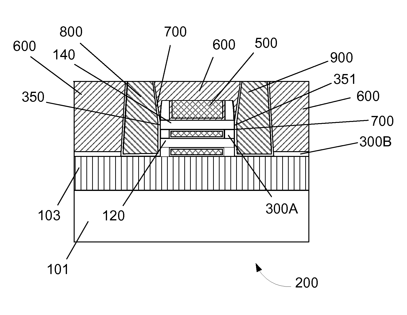
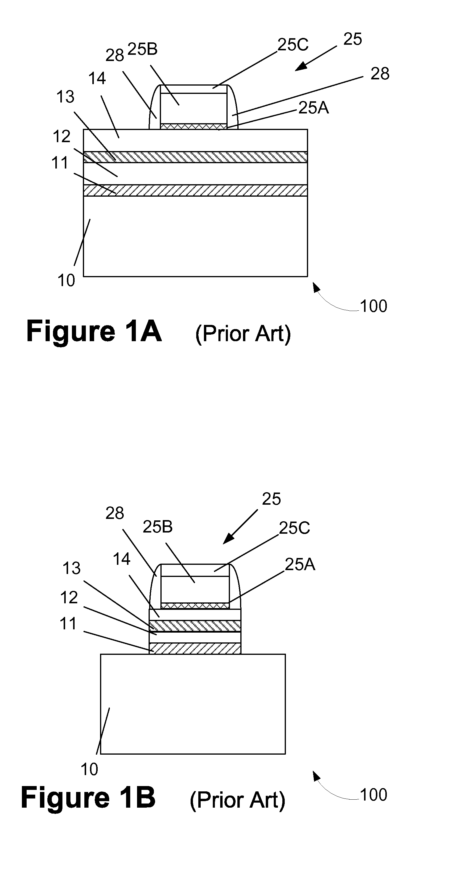
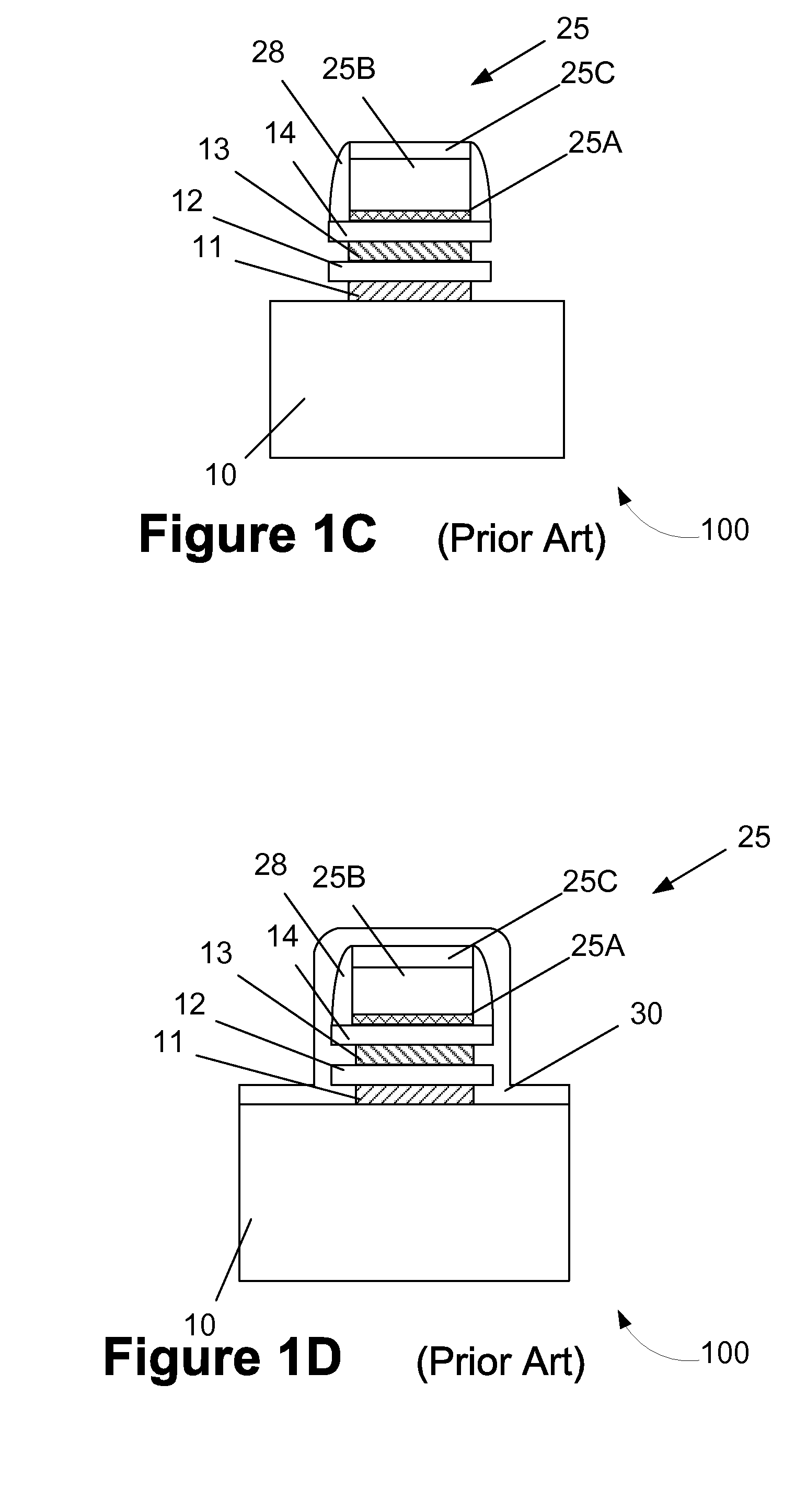
[0025]The present subject matter will now be described with reference to the attached figures. Various structures, systems, and devices are schematically depicted in the drawings for purposes of explanation only. The attached drawings are included to describe and explain illustrative examples of the present disclosure. The words and phrases used herein should be understood and interpreted to have a meaning consistent with the understanding of those words and phrases by those in the industry. No special definition of a term or phrase, i.e., a definition that is different from the ordinary and customary meaning as understood by those in the industry, is intended to be implied by consistent usage of the term or phrase herein. To the extent that a term or phrase is intended to have a special meaning, such a special definition will be expressly set forth in the specification in a definitional manner that directly and unequivocally provides the special definition for the term or phrase.

[0...


PUM


Abstract

A device includes a gate structure and a nanowire channel structure positioned under the gate structure. The nanowire channel structure includes first and second end surfaces. The device further includes a first insulating liner positioned on the first end surface and a second insulating liner positioned on the second end surface. The device further includes a metal-containing source contact positioned on the first insulating liner and a metal-containing drain contact positioned on the second insulating liner.

Description

BACKGROUND OF THE DISCLOSURE[0001]1. Field of the Disclosure[0002]The present disclosure generally relates to the formation of semiconductor devices and, more specifically, to various methods of forming nanowire devices with MIS (Metal-Insulator-Semiconductor) source / drain contacts and the resulting devices.[0003]2. Description of the Related Art[0004]The fabrication of advanced integrated circuits, such as CPUs (central processing units), storage devices, ASICs (application specific integrated circuits) and the like, requires the formation of a large number of circuit elements in a given chip area according to a specified circuit layout, wherein so-called metal oxide semiconductor field effect transistors (MOSFETs or FETs) represent one important type of circuit element that substantially determines performance of the integrated circuits. A FET is a planar device that typically includes a source region, a drain region, a channel region that is positioned between the source region a...

Claims


Application Information

Patent Timeline
IPC IPC(8): H01L29/775H01L21/768H01L29/66
CPCH01L29/775H01L21/76879H01L29/66439H01L29/517H01L29/1033B82Y10/00H01L29/41725H01L29/0673H01L21/76897H01L21/28512H01L29/42392H01L29/78696H01L29/40114H01L29/66545
Inventor BOUCHE, GUILLAUMEWAN, JINGWEI, ANDY C.KOH, SHAO-MING
Owner GLOBALFOUNDRIES INC
Why Eureka
Try Eureka