Cell string and reading method for the cell string

a cell string and reading method technology, applied in the field of cell string and reading method of the cell string, can solve the problem that the refresh margin cannot be increased, and achieve the effect of small threshold voltage distribution and good refresh margin

Active Publication Date: 2015-12-03
SEOUL NAT UNIV R&DB FOUND
View PDF5 Cites 7 Cited by
  • Summary
  • Abstract
  • Description
  • Claims
  • Application Information

AI Technical Summary

Benefits of technology

[0011]The invention is to provide a cell string capable of achieving a small distr

Problems solved by technology

As a result, a refresh ma

Method used


Image

  • Cell string and reading method for the cell string
  • Cell string and reading method for the cell string
  • Cell string and reading method for the cell string

Examples


first embodiment

[0052]Hereinafter, the above-described components of the invention will be described in detail.

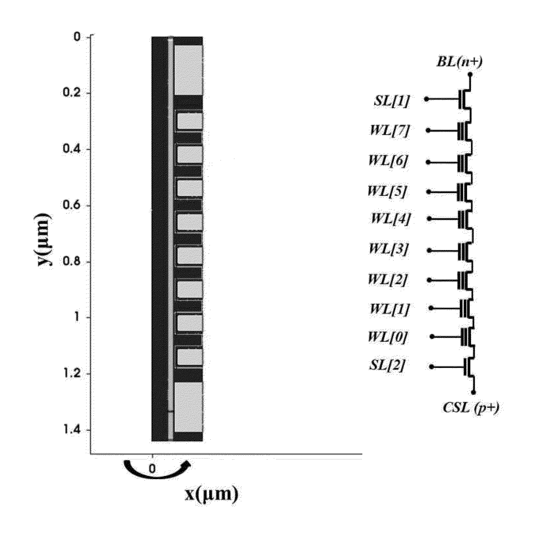
[0053]The insulating layer 510 is formed to have a cylindrical shape on a surface of the semiconductor substrate 500 in the vertical direction, and the semiconductor body 520 is formed on a surface of the insulating layer.

[0054]The cell string includes the diode configured with the first and second semiconductor region 530 and 540 arranged at the two ends of the semiconductor body 520. The first semiconductor region and the second semiconductor region are doped with opposite type impurities. The semiconductor body 520 is configured to include at least two layers521 and 522. Preferably, the layers of the semiconductor body are made of materials having different energy band gaps. The semiconductor body may be configured with an intrinsic semiconductor or may be configured to be doped with a low concentration of impurities. When a forward direction voltage is applied to the first and second s...

third embodiment

[0069]The reading method of the cell string according to the invention includes a pre-charging step and a reading step. In the embodiment, the pre-charging step may not be included. However, in terms of durability, it is preferable that the pre-changing step be included. The reading method according to the invention denotes a general read operation or denotes a verify operation after programming or erasing operation.

[0070]Hereinafter, the reading method according to the embodiment will be described in detail with reference to FIGS. 11 to 16. FIG. 11 is a graph illustrating states of bias applied to lines of a cell string for explaining a reading method according to the third embodiment of the invention. FIGS. 14A to 14E are energy band diagrams at steps t2, t3, t4, t6, and t7 of FIG. 11.

[0071]Referring to FIGS. 11 and 14A to 14E, the reading method for the cell string having the above-described structures according to the invention includes a pre-charging step and a reading step for...


PUM


Abstract

Provided are a cell string and a reading method for the cell string. The cell string includes a semiconductor body formed on a surface of an insulating layer, first and second semiconductor regions formed at respective ends of the semiconductor body and are formed by being doped with different types of impurities, two or more control electrodes which are separated from each other to be electrically isolated, and a gate insulating film stack which is formed between the semiconductor body and the control electrodes, wherein the semiconductor body is configured to include at least two layers, and adjacent layers of the semiconductor body have different energy band gaps, wherein the semiconductor body is formed by an intrinsic semiconductor or a semiconductor being doped with impurities, and wherein the first and second semiconductor regions are doped with impurities of which concentration is higher than that of the semiconductor body.

Description

CROSS-REFERENCE TO RELATED PATENT APPLICATION[0001]This application claims the benefit of Korean Patent Application No. 10-2014-0065533, filed on May 30, 2014 in the Korean Intellectual Property Office, the disclosure of which is incorporated herein in its entirety by reference.BACKGROUND OF THE INVENTION[0002]1. Field of the Invention[0003]The present invention relates to a cell string and a reading method for the cell string, and more particularly, to a cell string wherein a semiconductor body where a channel is formed includes at least two or more layers and adjacent layers are made of materials having different energy band gaps to increase a turn-on current, using positive feedback to obtain steep switching characteristic, and capable of reducing distribution of a turn-on voltage and a reading method for the cell string.[0004]2. Description of the Related Art[0005]Various researches have been made in order to improve a degree of integration and performance of a flash memory devi...

Claims


Application Information

Patent Timeline
IPC IPC(8): G11C16/26H01L29/78H01L27/12H01L27/115H01L29/06G11C16/04H01L29/423
CPCG11C16/26G11C16/0483H01L29/7827H01L29/7841H01L27/11582H01L29/7831H01L27/11556H01L29/0649H01L27/1203H01L29/42356G11C11/5642H10B43/35H10B43/27H10B41/30H10B41/27
Inventor LEE, JONG-HOJOE, SUNG-MIN
Owner SEOUL NAT UNIV R&DB FOUND
Why Eureka
Try Eureka