
Eureka
For R&D, Eureka makes reading and utilizing patents & technical documents easy.
Eureka AIR
Designed for self-driven R&D workflows. Generate viable solutions, solve complex R&D challenges, empower your innovation with AI.

Eureka Materials
Designed for material experts only. Revolutionize your material R&D, from search, analyze, to developing new materials.

TechResearch
Generate reliable direction feasibility study reports for your R&D in just a few steps.

TechSeek
Discover and master advanced knowledge NOW. Basics, ideas, possibilities, all at once.

TechMind
As an expert in R&D Theories, TechMind can generates customized viable solutions instantly.

TechRisk
Analyze your overall solution with one click, know your potential R&D risks in advance.

TechMonitor
Get weekly tech updates, stay abreast of the latest tech innovations and key insights.
Method for manufacturing optical element
- Summary
- Abstract
- Description
- Claims
- Application Information
AI Technical Summary
Benefits of technology
Problems solved by technology
Method used
Image

Examples
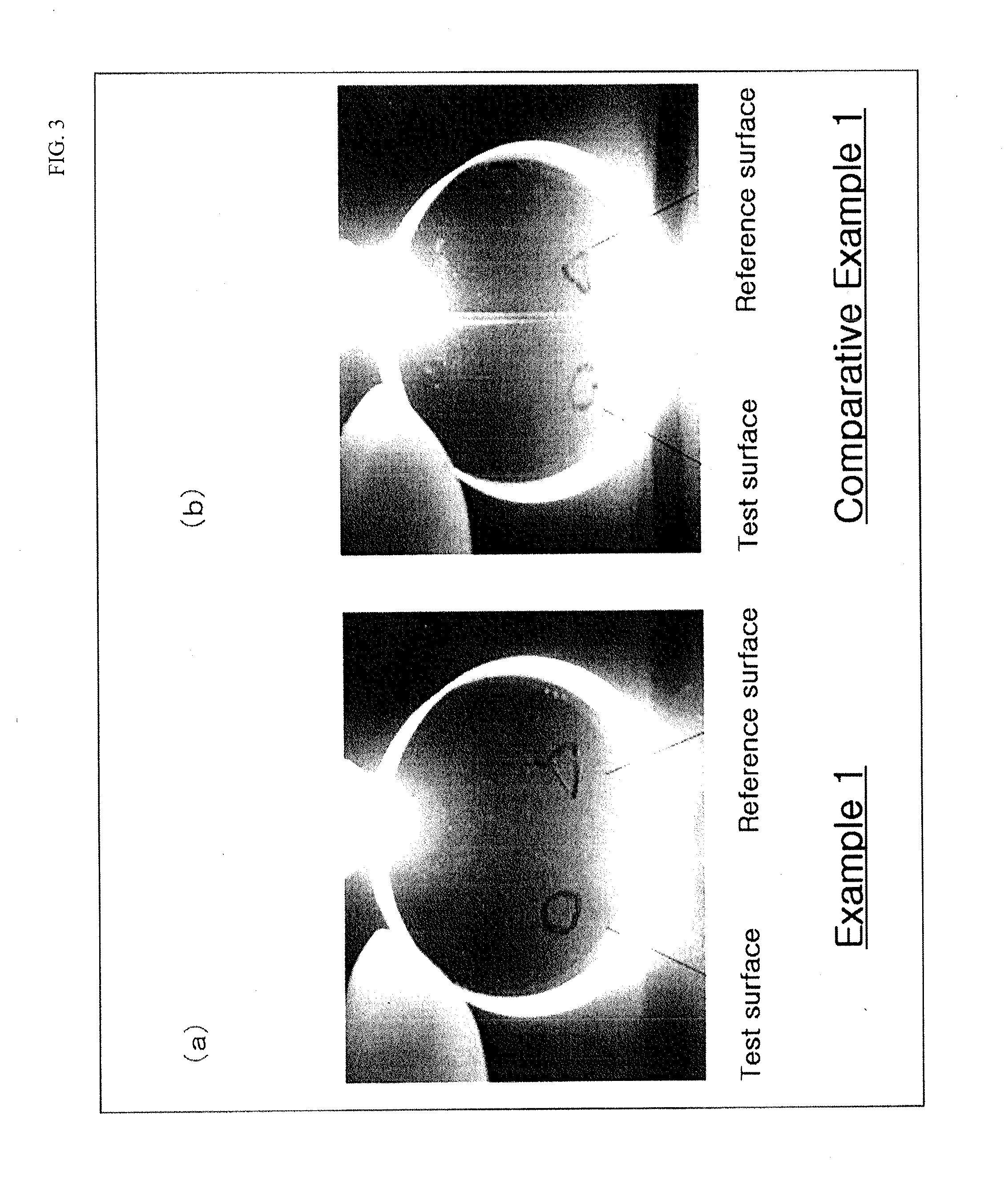
example 1
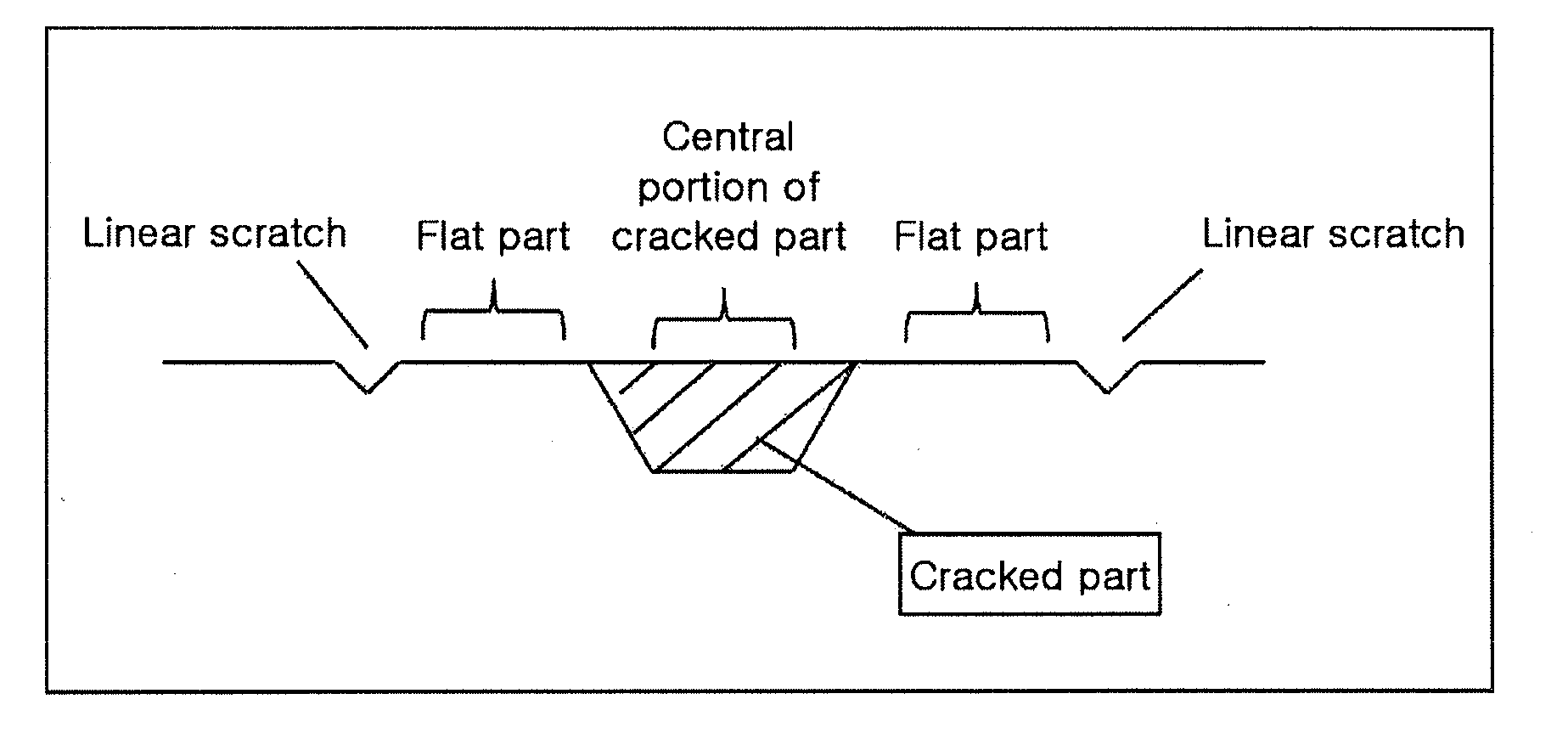
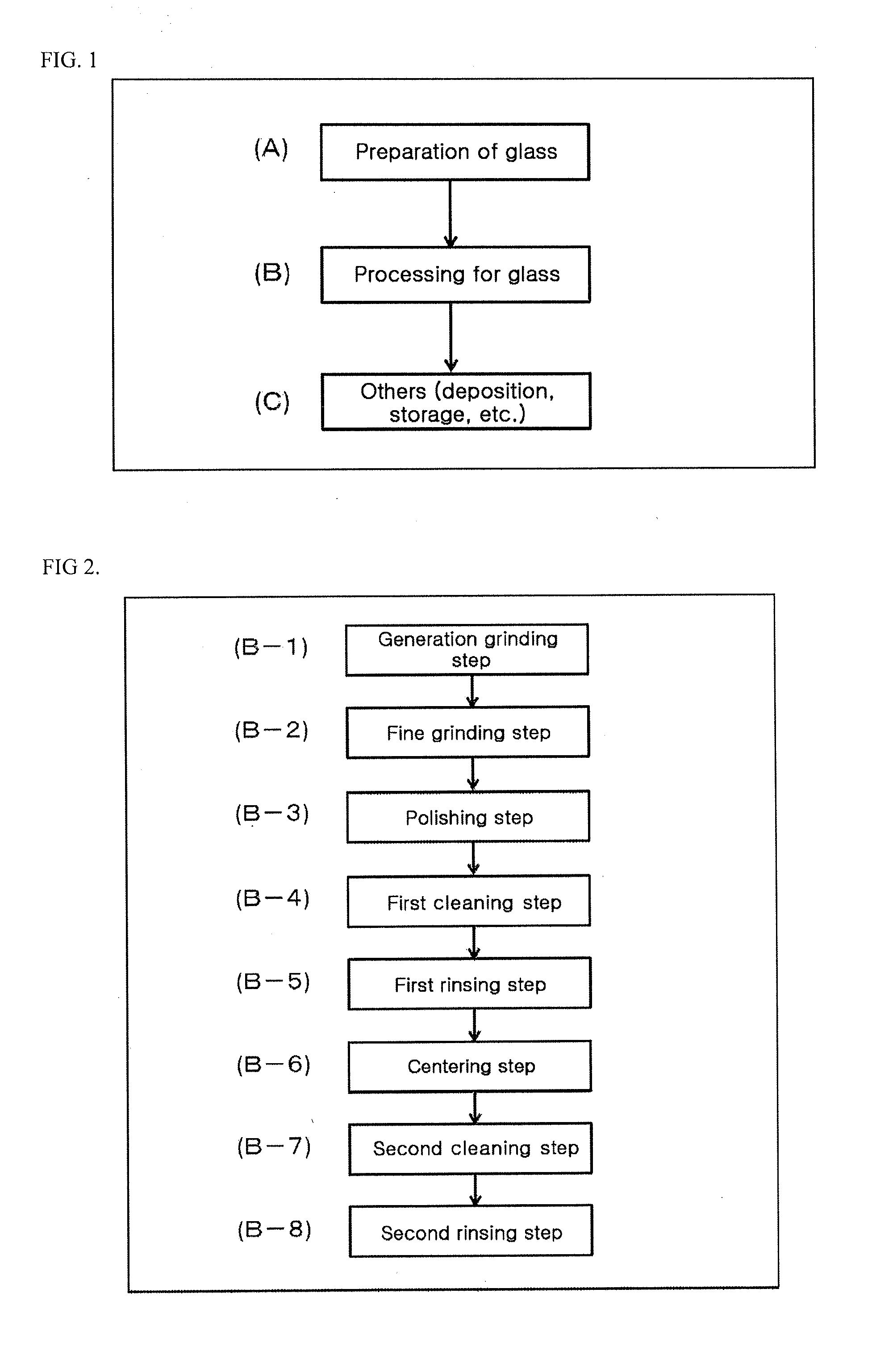
[0134]First, a disc-shaped plane glass substrate (diameter of 43.7 mm and thickness of 5 mm) was used as glass. This plane substrate was previously polished. Further, the glass 1 illustrated in the above-described exemplary embodiment was used as a glass material of the glass substrate. The cleaning after the polishing was performed by manually wiping the glass by the lens paper using the organic solvent.
[0135]Then, masking was performed by attaching tape to a portion of the glass substrate. After the masking was performed, the glass substrate was immersed in the rinsing liquid. In other words, a portion subjected to the masking becomes a reference surface that is not affected by the rinsing liquid. A portion of the glass substrate that is in contact with the rinsing liquid becomes a test surface. It is possible to confirm the degree of change in quality of a main surface of the glass substrate by comparing the test surface with the reference surface after the tape is detached there...
example 2
[0181]In Example 2, the above-described glass 2 was used as the glass material of the glass substrate. The glass substrate was manufactured while other conditions remaining the same as Example 1.
PUM
| Property | Measurement | Unit |
|---|---|---|
| Diameter | aaaaa | aaaaa |
| Acidity | aaaaa | aaaaa |
| Content | aaaaa | aaaaa |
Abstract
Description
Claims
Application Information
 - R&D Engineer
- R&D Manager
- IP Professional
- Industry Leading Data Capabilities
- Powerful AI technology
- Patent DNA Extraction
Browse by: Latest US Patents, China's latest patents, Technical Efficacy Thesaurus, Application Domain, Technology Topic, Popular Technical Reports.
© 2024 PatSnap. All rights reserved.Legal|Privacy policy|Modern Slavery Act Transparency Statement|Sitemap|About US| Contact US: help@patsnap.com