Semiconductor device

a technology of semiconductor devices and solder joints, applied in semiconductor devices, semiconductor/solid-state device details, electrical devices, etc., can solve problems such as cracks at the boundary of sealing resin and solder, and achieve the effect of preventing cracks

Active Publication Date: 2015-12-10
DENSO CORP
View PDF0 Cites 1 Cited by
  • Summary
  • Abstract
  • Description
  • Claims
  • Application Information

AI Technical Summary

Benefits of technology

[0006]When current flows and thus a temperature rises in the semiconductor device including the sealing resin and the solder, a crack might occur at a boundary of the sealing resin and the solder, due to a difference between the sealing resin and the solder in thermal expansion coefficient. The crack that has occurred might develop toward an inner side and reach a boundary of the metal film and the insulation film. In an occurrence of such a crack, since the semiconductor device described above includes the insulation film having the convex protruding toward the metal film and the metal film covers the convex, the crack developing through the boundary of the metal film and the insulation film stops at the convex. This structure can prevent the crack from developing.

Problems solved by technology

When current flows and thus a temperature rises in the semiconductor device including the sealing resin and the solder, a crack might occur at a boundary of the sealing resin and the solder, due to a difference between the sealing resin and the solder in thermal expansion coefficient.

Method used


Image

  • Semiconductor device
  • Semiconductor device
  • Semiconductor device

Examples


Embodiment Construction

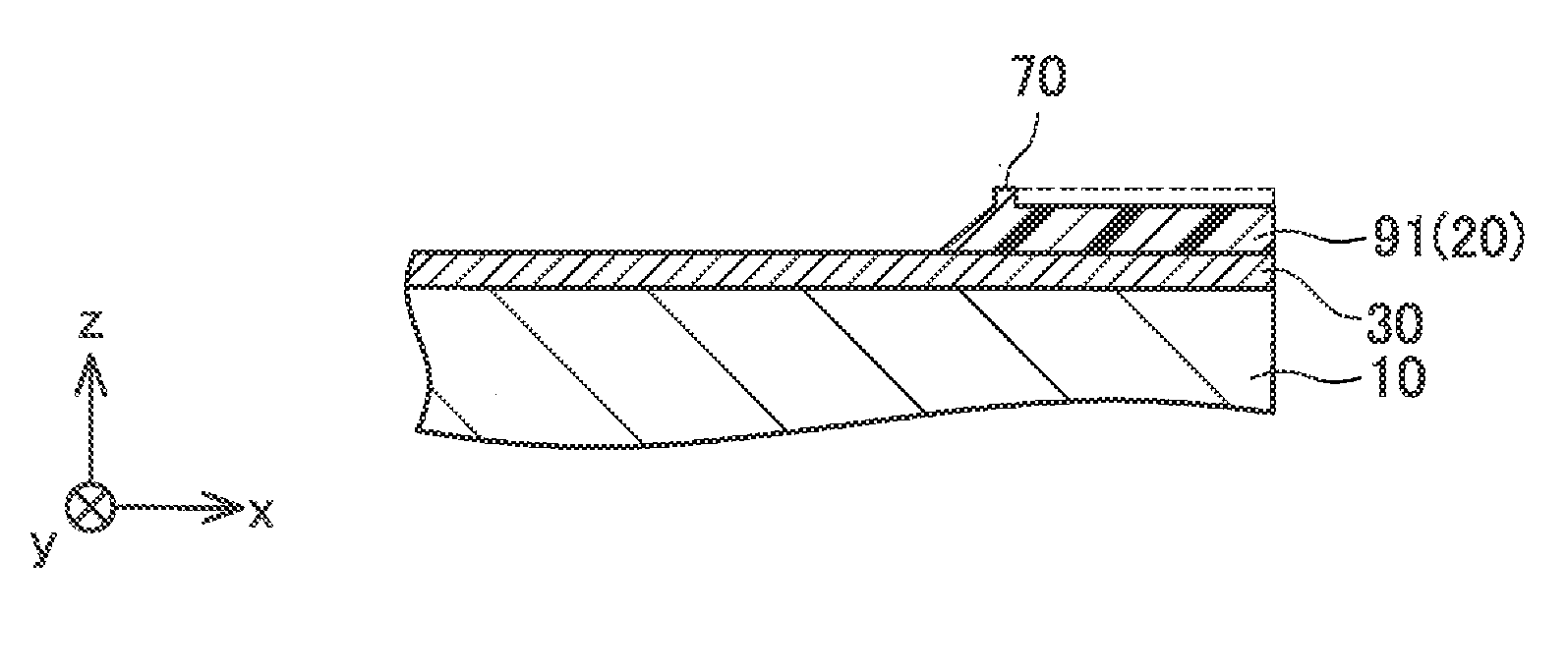
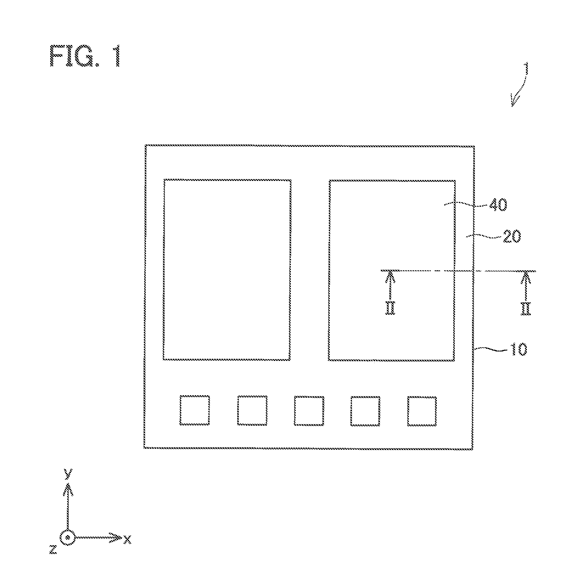
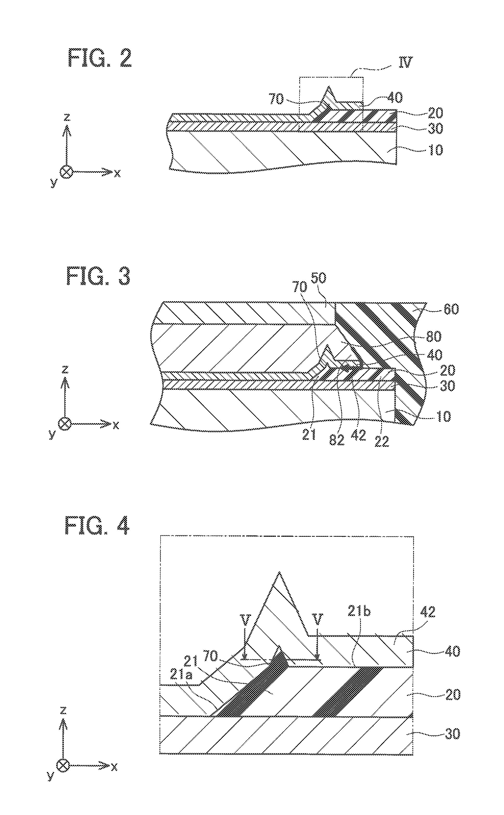
[0021]An embodiment will be described below with reference to the attached drawings. As illustrated in FIG. 1 and FIG. 2, a semiconductor device 1 includes a semiconductor substrate 10, an electrode 30 formed on a surface of the semiconductor substrate 10, an insulation film 20 formed on a surface of the electrode 30, and a metal film 40 formed on t he surface of the electrode 30 and a surface of the insulation film 20. As illustrated in FIG. 3, the semiconductor device 1 further includes a lead frame 50 joined to the metal film 40 by solder 80 and sealing resin 60 sealing an entire structure. In FIG. 1 and FIG. 2, the solder 80, the lead frame 50, and the sealing resin 60 are omitted.

[0022]The semiconductor substrate 10 is made of silicon (Si). As other examples, the semiconductor substrate 10 may be made of silicon carbide (SiC), gallium nitride (GaN), and the like. A semiconductor element (not shown) is formed within the semiconductor substrate 10. An insulated gate bipolar trans...


PUM

PropertyMeasurementUnit
temperatureaaaaaaaaaa
stressaaaaaaaaaa
thermal expansion coefficientaaaaaaaaaa

Abstract

A semiconductor device 1 is provided with a semiconductor substrate 10, an electrode 30 formed on a surface of the semiconductor substrate 10, and an insulation film 20 formed on the electrode 30. The semiconductor device 1 includes a metal film 40 extending over a part of the surface of the electrode 30 not covered by the insulation film 20 and a surface of the insulation film 20. The semiconductor device 1 includes solder 80 formed on a surface of the metal film 40, a lead frame 50 joined to the metal film 40 by the solder 80, and sealing resin 60 sealing the insulation film 20, the metal film 40, and the solder 80. A convex 70 is formed on the surface of the insulation film 20. The metal film 40 covers the convex 70. The solder 80 covers the metal film 40 covering the convex 70.

Description

CROSS-REFERENCE TO RELATED APPLICATION[0001]This application claims priority to Japanese Patent Application No. 2014-118492 filed on Jun. 9, 2014, the contents of which are hereby incorporated by reference into the present application.TECHNICAL FIELD[0002]The present application relates to a semiconductor device.DESCRIPTION OF RELATED ART[0003]When current flows through and thus a temperature rises in a semiconductor device including a solder layer, a crack may occur in the solder layer due to stress. Japanese Patent Application Publication No. 2013-214561 (JP 2013-214561 A) discloses a technique of preventing the crack from occurring and developing in a solder layer in a semiconductor device. According to the technique disclosed in JP 2013-214561 A, the solder layer is composed of a solid-solubilized-hardening type solder material including Sn as a major component and solid-solubilized elements being solid-solubilized into this Sn.[0004]The technique disclosed in JP 2013-214561 A p...

Claims


Application Information

Patent Timeline
Patent Type & Authority Applications(United States)
IPC IPC(8): H01L23/00H01L23/31H01L23/495
CPCH01L23/562H01L23/49513H01L23/49586H01L2224/32245H01L23/3157H01L24/32H01L2924/07025H01L23/49541H01L23/49562H01L24/03H01L24/05H01L24/29H01L24/83H01L2224/0345H01L2224/0346H01L2224/04026H01L2224/05557H01L2224/05558H01L2224/05647H01L2224/05655H01L2224/0603H01L2224/291H01L2224/29111H01L2224/83447H01L2224/83801H01L2924/13055H01L2924/13091H01L2924/3512H01L2924/00H01L2924/014H01L2924/00014H01L2924/01047H01L2924/01029
Inventor FUKAMI, TAKESHI
Owner DENSO CORP
Why Eureka
Try Eureka