Substrate with electronic device embedded therein and manufacturing method thereof

Inactive Publication Date: 2015-12-17
SAMSUNG ELECTRO MECHANICS CO LTD
View PDF1 Cites 1 Cited by
  • Summary
  • Abstract
  • Description
  • Claims
  • Application Information

AI Technical Summary

Benefits of technology

[0010]Some embodiments of the present invention provide an electronic device embedded substrate

Problems solved by technology

Although forming a large cavity would be advantageous for embedding the electronic device in the cavity, forming the cav

Method used


Image

  • Substrate with electronic device embedded therein and manufacturing method thereof
  • Substrate with electronic device embedded therein and manufacturing method thereof
  • Substrate with electronic device embedded therein and manufacturing method thereof

Examples


Example

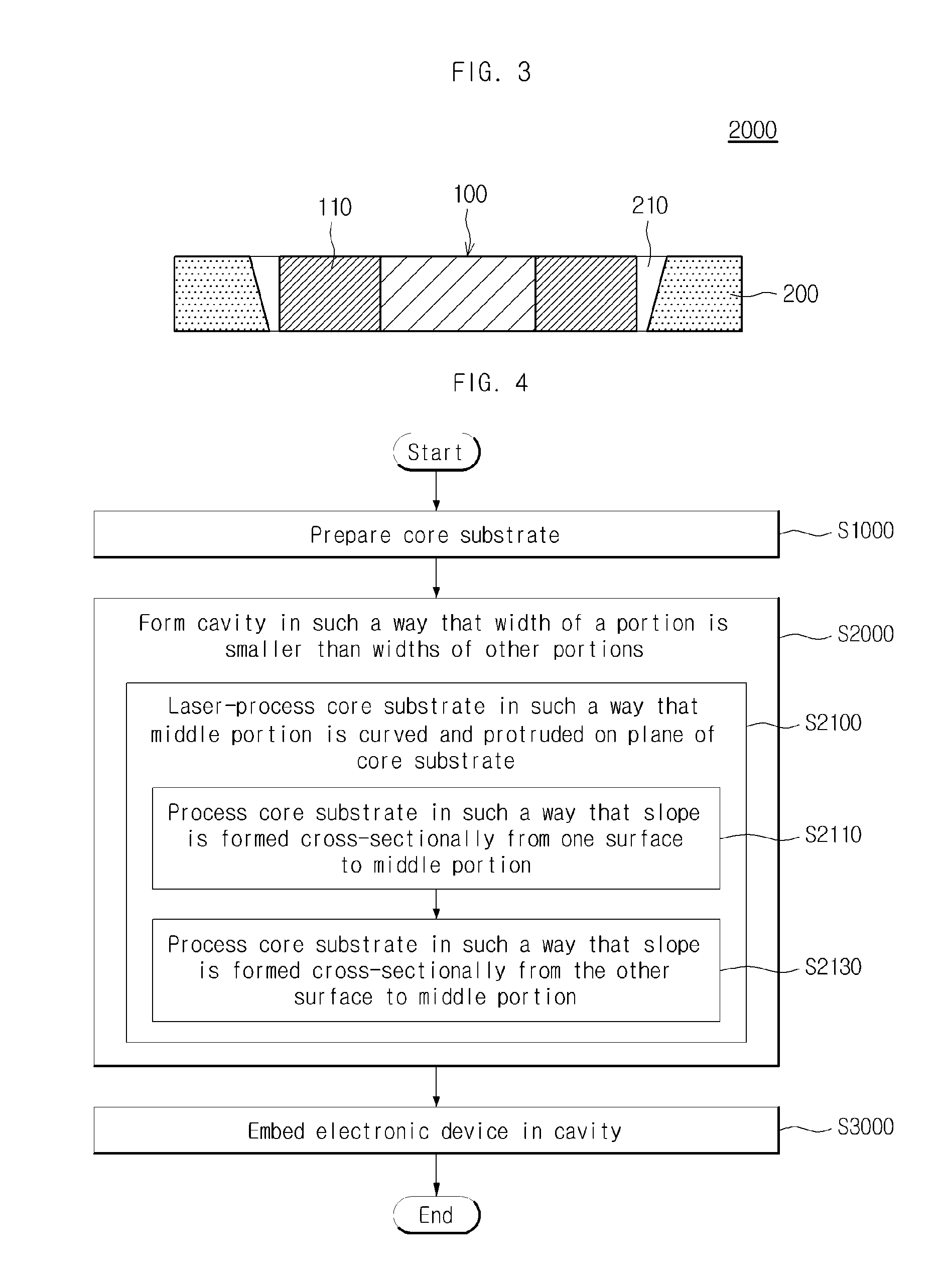
[0024]Hereinafter, an electronic device embedded substrate and a method of manufacturing the same in accordance with certain embodiments of the present invention will be described in detail with reference to the accompanying drawings. In describing the present invention with reference to the accompanying drawings, any identical or corresponding elements will be assigned with same reference numerals, and no redundant description thereof will be provided.

[0025]When one element is described to be “coupled” to another element, it does not refer to a physical, direct contact between these elements only, but it shall also include the possibility of yet another element being interposed between these elements and each of these elements being in contact with said yet another element.

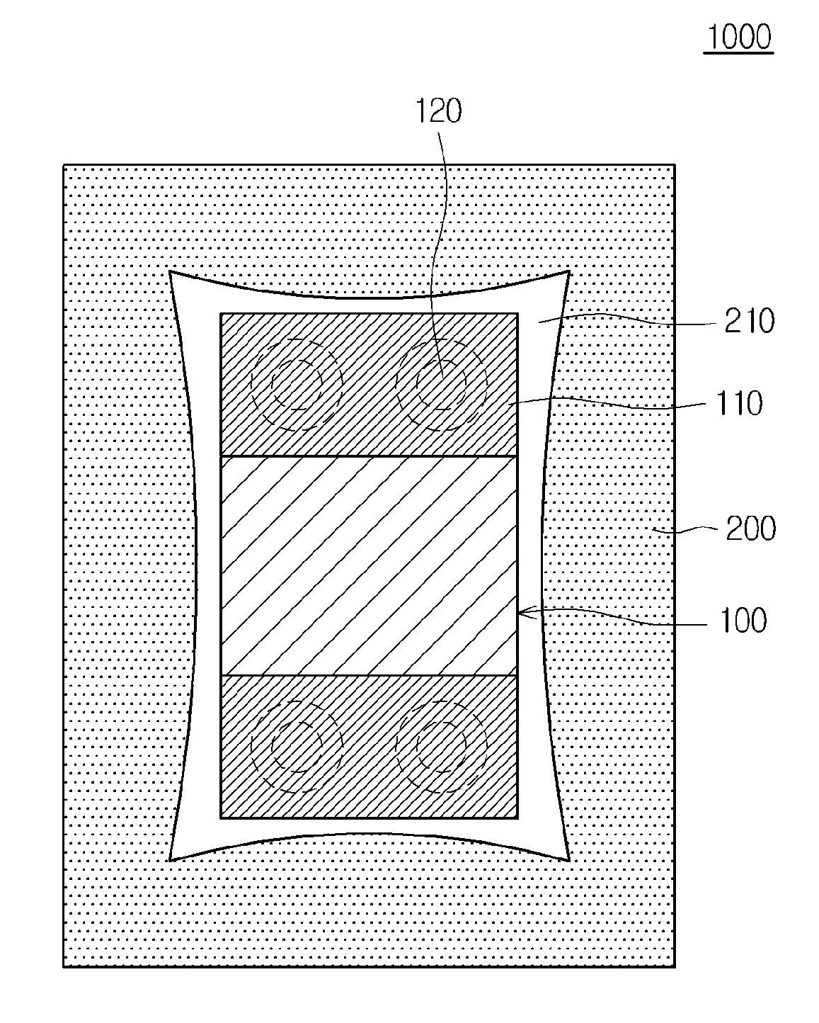
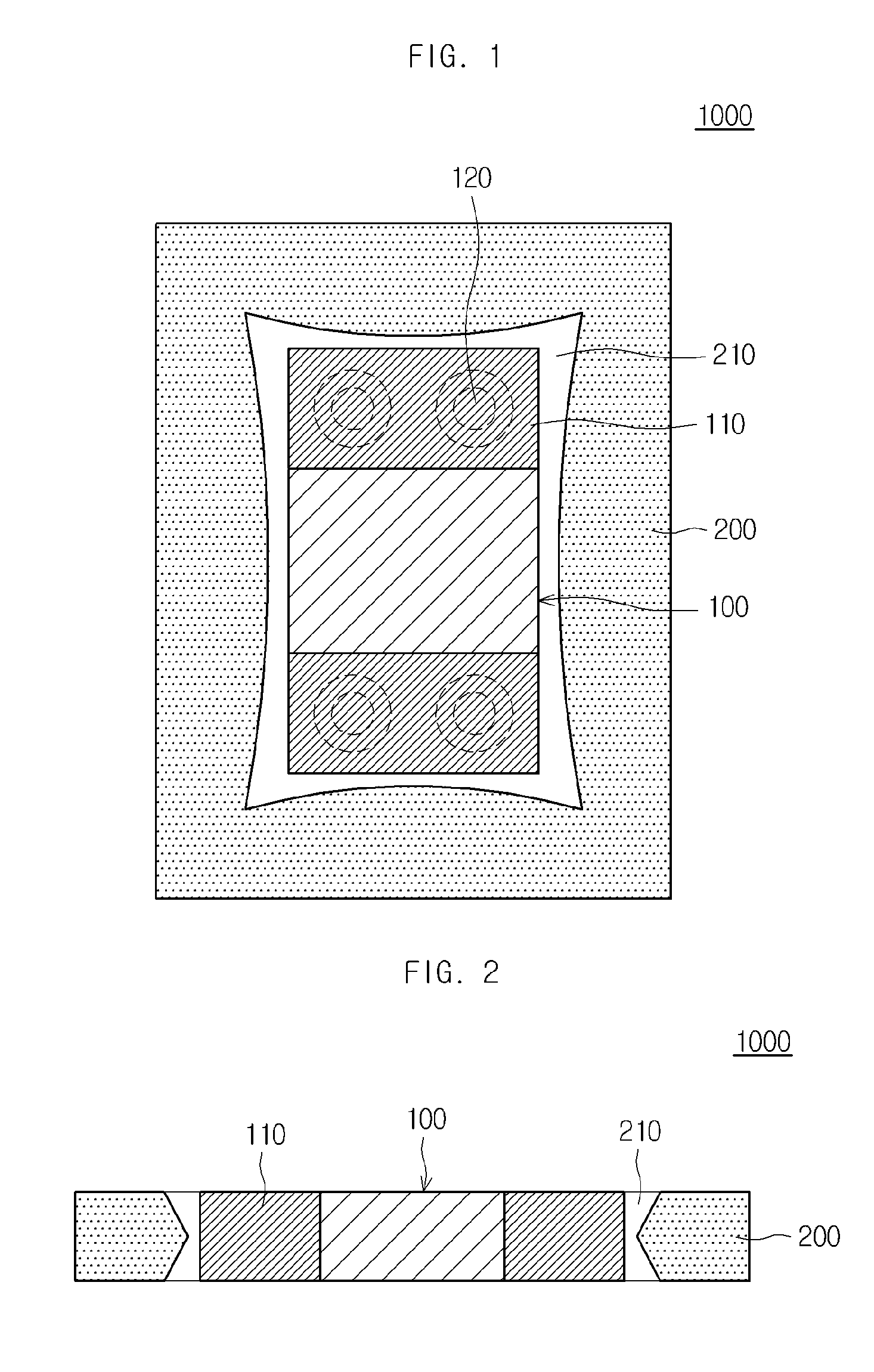
[0026]FIG. 1 is a top view showing an electronic device embedded substrate in accordance with an embodiment of the present invention. FIG. 2 is a cross-sectional view showing the electronic device embedded substr...


PUM

PropertyMeasurementUnit
Widthaaaaaaaaaa

Abstract

An electronic device embedded substrate and a method of manufacturing the same are disclosed. The electronic device embedded substrate in accordance with an aspect of the present invention includes: an electronic device; and a core substrate having a cavity, in which the electronic device is embedded and of which a width of at least a portion is smaller than widths of other portions thereof.

Description

CROSS-REFERENCE TO RELATED APPLICATIONS[0001]This application claims the benefit of Korean Patent Application No. 10-2014-0073584, filed with the Korean Intellectual Property Office on Jun. 17, 2014, the disclosure of which is incorporated herein by reference in its entirety.BACKGROUND[0002]1. Technical Field[0003]The present invention relates to an electronic device embedded substrate and a manufacturing method thereof.[0004]2. Background Art[0005]In the conventional electronics manufacturing industry, most active / passive elements have been mounted over a substrate by use of the surface mount technology (SMT). However, in step with the electronic products that have been increasingly smaller, new packing technologies have been developed to embed the active / passive elements in the substrate.[0006]In the case of active / passive element embedded substrate products, economical manufacturing processes are possible by integrating various active / passive elements in organic substrates, and t...

Claims


Application Information

Patent Timeline
IPC IPC(8): H05K1/18H05K3/00H05K3/30
CPCH05K1/182H05K3/30Y10T29/49131H05K2201/10015H05K2201/1003H05K3/0026H05K1/0271H05K1/185H05K2201/09072H05K2201/09827H05K2201/09854H05K1/18H05K3/46
Inventor KIM, TAE-SEONGYU, YEON-SEOPLEE, BOK-HEE
Owner SAMSUNG ELECTRO MECHANICS CO LTD
Why Eureka
Try Eureka