

Semiconductor device having vertical channel, resistive memory device including the same, and method of manufacturing the same
a technology of resistive memory and semiconductors, applied in the direction of semiconductor devices, bulk negative resistance effect devices, electrical appliances, etc., can solve the problem that the study of existing electronic charge-controlled devices may encounter limitations
- Summary
- Abstract
- Description
- Claims
- Application Information
AI Technical Summary
Benefits of technology
Problems solved by technology
Method used
Image

Examples
Embodiment Construction
”.
BRIEF DESCRIPTION OF THE DRAWINGS
[0016]Embodiments will be more clearly understood from the following detailed description taken in conjunction with accompanying drawings, in which:
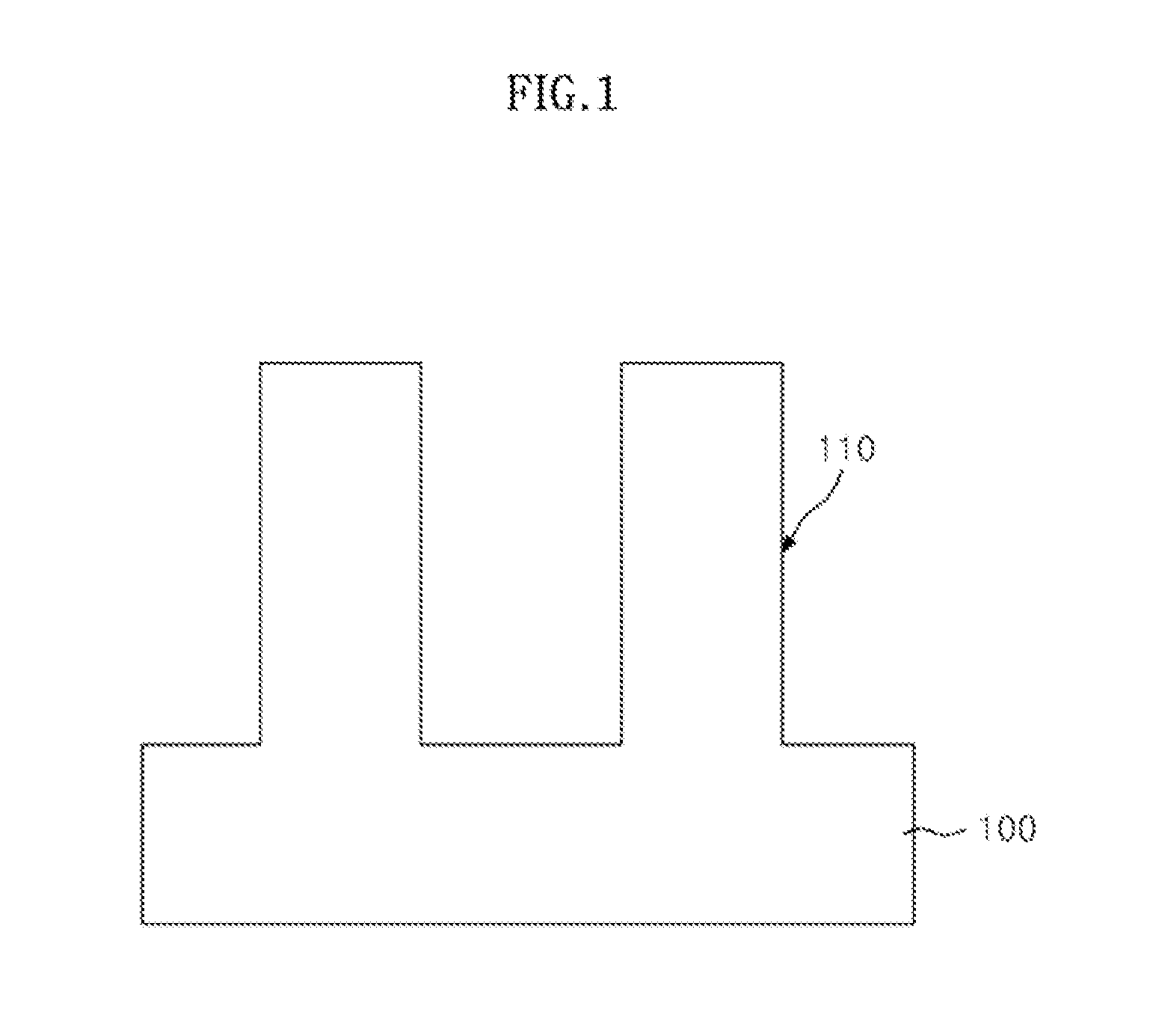
[0017]FIG. 1 is cross-sectional view illustrating a method of manufacturing a semiconductor device having a vertical channel according to an embodiment;
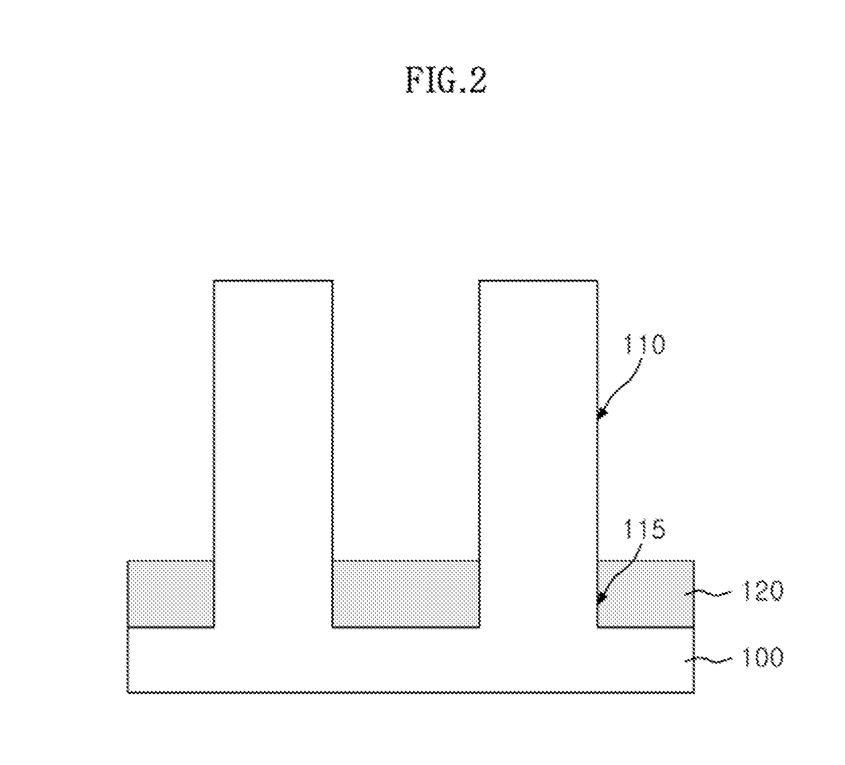
[0018]FIG. 2 is cross-sectional view illustrating a method of manufacturing a semiconductor device having a vertical channel according to an embodiment;
[0019]FIG. 3 is cross-sectional view illustrating a method of manufacturing a semiconductor device having a vertical channel according to an embodiment;
[0020]FIG. 4 is cross-sectional view illustrating a method of manufacturing a semiconductor device having a vertical channel according to an embodiment;
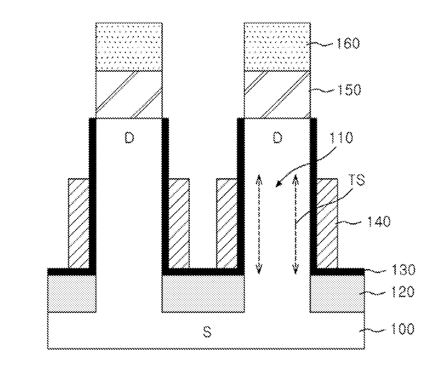
[0021]FIG. 5 is a cross-sectional view illustrating a resistive memory device including a semiconductor device having a vertical channel according to an embodiment.
DETAILED DESCRIPTION
[0022]Hereinafter exem...
PUM
 Abstract
Description
Claims
Application Information