Optical device and method for manufacturing same

a technology of optical devices and manufacturing methods, applied in the field of optical devices, can solve the problems of shortening the life of the optical device chip, degrading the reflection capability of light, and not being an efficient improvement measure, and achieves the effects of reducing the infiltration of moisture, and reducing the infiltration rate of moistur

Active Publication Date: 2015-12-24
POINT ENG
View PDF1 Cites 1 Cited by
  • Summary
  • Abstract
  • Description
  • Claims
  • Application Information

AI Technical Summary

Benefits of technology

[0032]As described above, an optical device and a method for manufacturing same according to an exemplary embodiment of the present invention can obtain a more superior sealing power by suggesting a structure and a method wherein a portion of the sealant to be bonded to the metal plated layer is directly bonded to the metal substrate, in other words, by directly bonding the sealant to the aluminum metal substrate having a more superior bonding strength than the metal plated layer at the edge or the peripheral region thereof where the sealant is bonded to the metal plated layer. Accordingly, the present invention minimizes the infiltration of moisture or hazardous gases into the shielding sealant therefore it may bring the effect that the optical reflection property can be consistently maintained by preventing discoloration of the metal plated layer caused by the hazardous gases and the like.
[0033]In addition, the present invention may also bring the effect that the lifetime of an optical device may be extended by blocking the infiltration of hazardous substances into the sealant by tightly sealing the optical device through direct bonding of the aluminum metal substrate with the sealant.

Problems solved by technology

However, such method may not be an efficient improvement measure since it requires process equipments and high processing cost.
Consequently, such effect of discoloration will degrade the reflection capability of the light.
Moreover, it may result in the shortening of the lifetime of the optical device chip 40 due to the infiltrated hazardous gases or moisture.

Method used


Image

  • Optical device and method for manufacturing same
  • Optical device and method for manufacturing same
  • Optical device and method for manufacturing same

Examples


Embodiment Construction

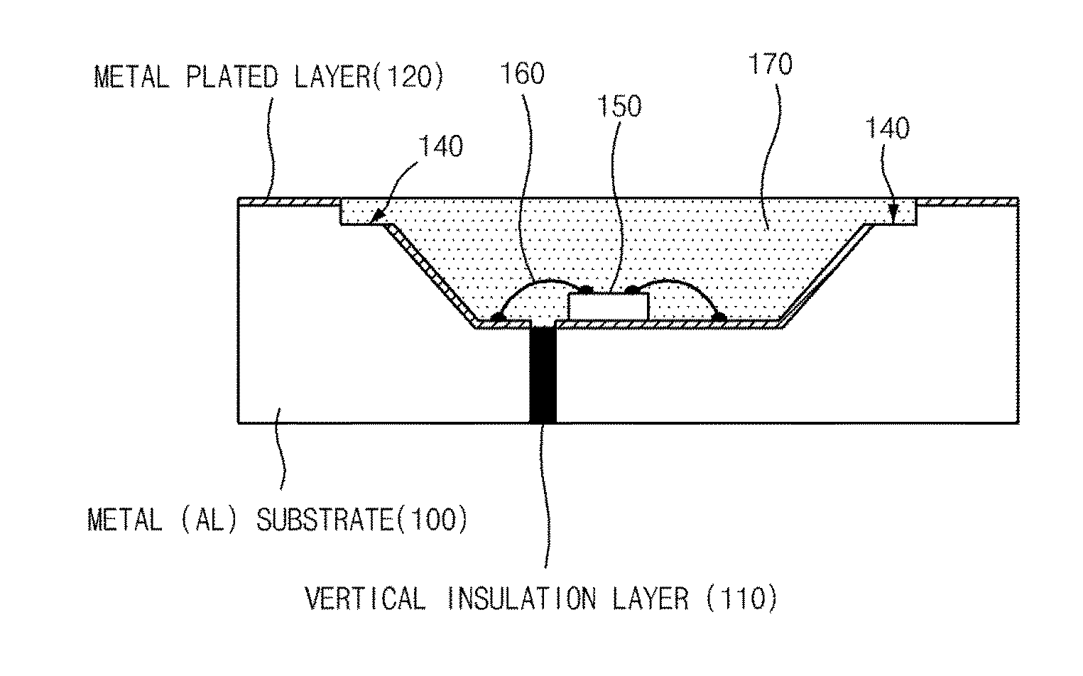
[0041]Hereinafter, an optical device and a method for manufacturing same according to an exemplary embodiment of the present invention will be described in detail with reference to the accompanying drawings.

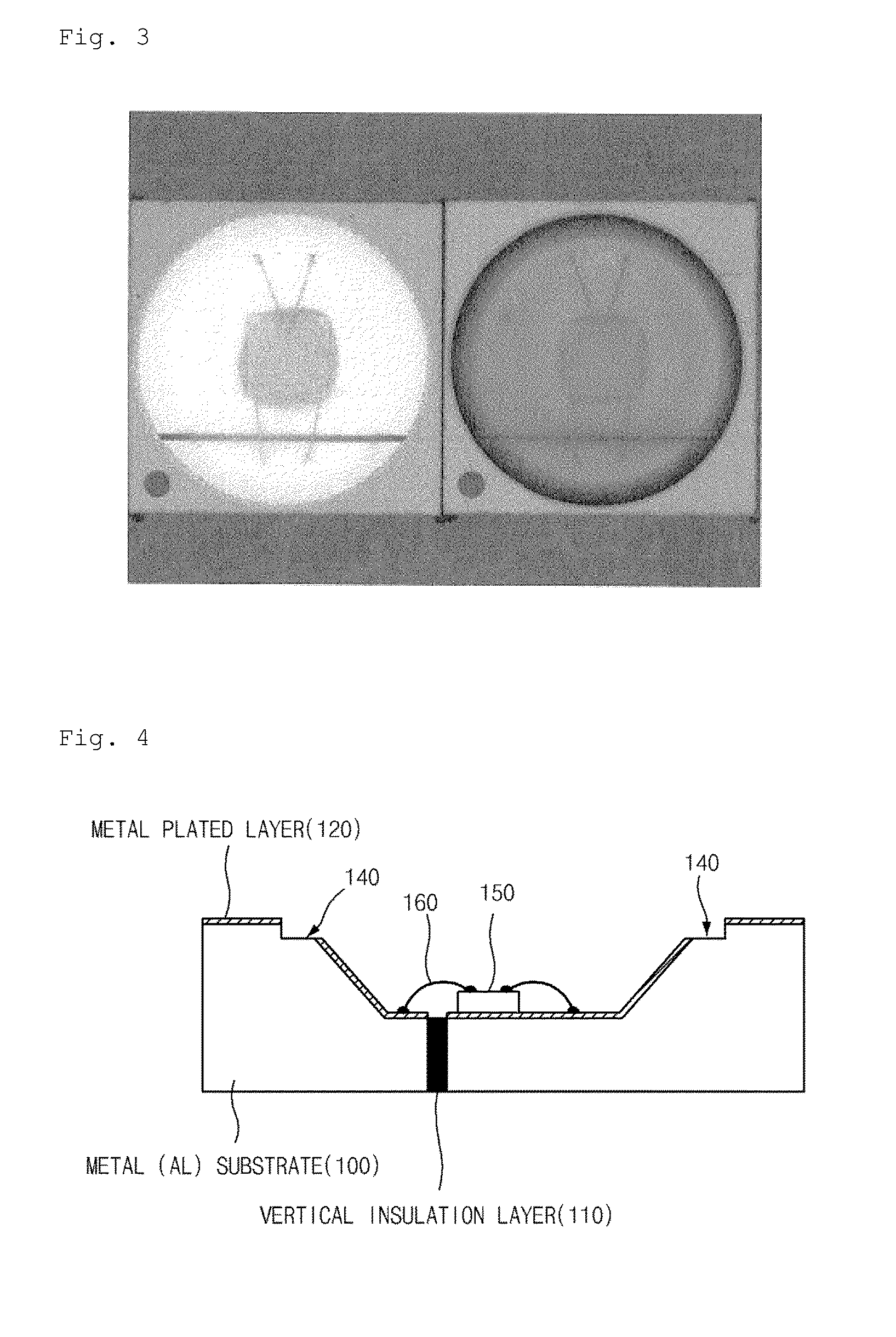
[0042]FIGS. 4 and 5 are the exemplary drawings illustrating the cross-sections of the optical devices according to an exemplary embodiment of the present invention. Hereinafter, a structure of an optical device along with a method for manufacturing same will be described.

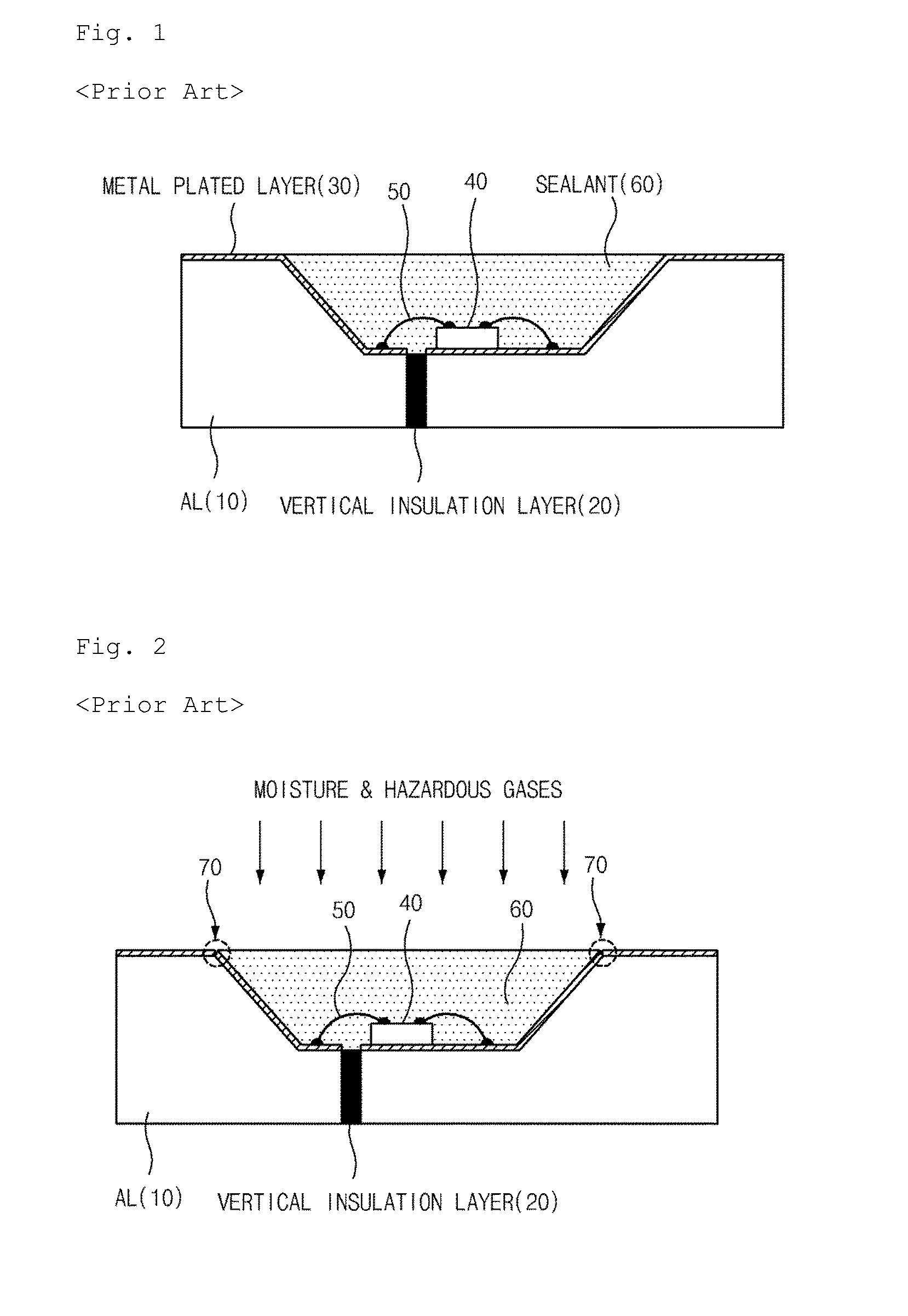
[0043]Referring to FIG. 4, firstly, an aluminum (Al) metal substrate 100 wherein a vertical insulation layer 110 is prepared for manufacturing of a cavity type optical device according to an exemplary embodiment of the present invention. Foresaid aluminum (Al) metal substrate 100 is a metal substrate having superior heat transfer characteristics and may also be made of an aluminum alloy. Description about the forming method of a vertical insulation layer 110 penetrating the metal substrate 100 from the upper surf...


PUM

PropertyMeasurementUnit
depthaaaaaaaaaa
distanceaaaaaaaaaa
adhesive strengthaaaaaaaaaa

Abstract

An optical device includes a metal substrate wherein at least one vertical insulation layer is formed from the upper to the lower surface; a metal plated layer formed on the upper surface of the metal substrate except for the vertical insulation layer; and an optical device chip bonded to one portion of the metal plated layer. One electrode of the optical device chip is electrically connected to a bonded surface of the metal plated layer, and the other electrode of the optical device chip is wire bonded to the other portion of metal plated layer. The optical device chip and a peripheral region thereof is shielded with a sealant, and at least one groove is formed on a partial surface of the metal plated layer so that a portion of the sealant is directly bonded to the metal substrate.

Description

TECHNICAL FIELD[0001]The present invention relates to an optical device, more particularly to an optical device for enhancing the adhesive strength between the sealant material and the metal substrate and a method for manufacturing same.BACKGROUND ART[0002]Semiconductor light emitting diode (LED), which is one of the optical devices, is receiving attention from various fields as an environment friendly light source. Recently, as applications of LEDs are expanding to various fields such as interior and exterior illuminations, automobile headlights, and back-light units (BLU) of the display devices, there are needs for high optical efficiency and excellent heat radiation characteristics of the LEDs. For high efficiency LEDs, materials or structures of the LEDs should be improved primarily, however, also there is a need for the improvement of the structures of the LED packages, the materials used therein, and the like.[0003]FIGS. 1 and 2 are the exemplary illustrations of the cross-sec...

Claims


Application Information

Patent Timeline
Patent Type & Authority Applications(United States)
IPC IPC(8): H01L33/62H01L33/54
CPCH01L33/54H01L33/62H01L2224/48091H01L2924/00014H01L33/48
Inventor AHN, BUM MOPARK, SEUNG HOSONG, TAE HWAN
Owner POINT ENG
Why Eureka
Try Eureka