Touch panel

a technology of touch panel and printing layer, applied in the direction of printed circuit stress/warp reduction, circuit optical details, instruments, etc., can solve the problems of affecting the insulating layer, and the deterioration of reliability, so as to achieve the alignment of the second sensing electrode and the insulating layer. , the effect of reducing the difficulty of the bridge electrod

Inactive Publication Date: 2015-12-24
LG INNOTEK CO LTD
View PDF1 Cites 12 Cited by
  • Summary
  • Abstract
  • Description
  • Claims
  • Application Information

AI Technical Summary

Problems solved by technology

For example, in the case of the high surface roughness, when an electrode is provided on the printing layer, an electrode may be damaged by protrusions of a printing layer.
However, as the sensing electrode is connected with the wire electrode provided on the printing layer, the sensing electrode is shorted due to the step difference resulting from the height of the printing layer, so that the reliability may be deteriorated.
In this case, the alignment of the second sensing electrode, the insulating layer, and the bridge electrode may be difficult.
In particular, a material, such as polyethylene terephthalate (PET), weak against heat may have a limitation in a heating temperature.

Method used


Image

  • Touch panel
  • Touch panel
  • Touch panel

Examples


Embodiment Construction

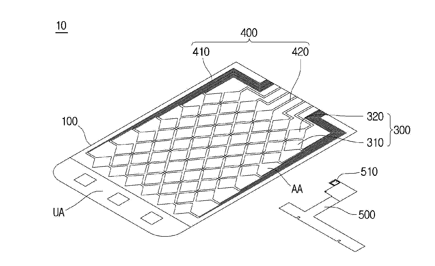
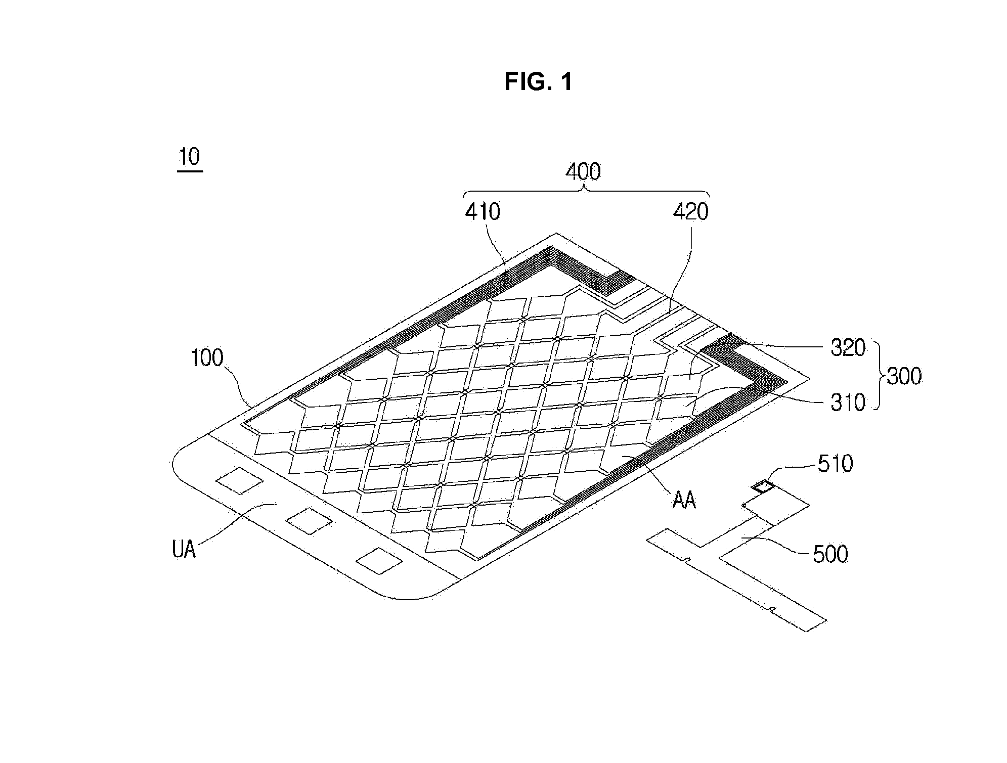
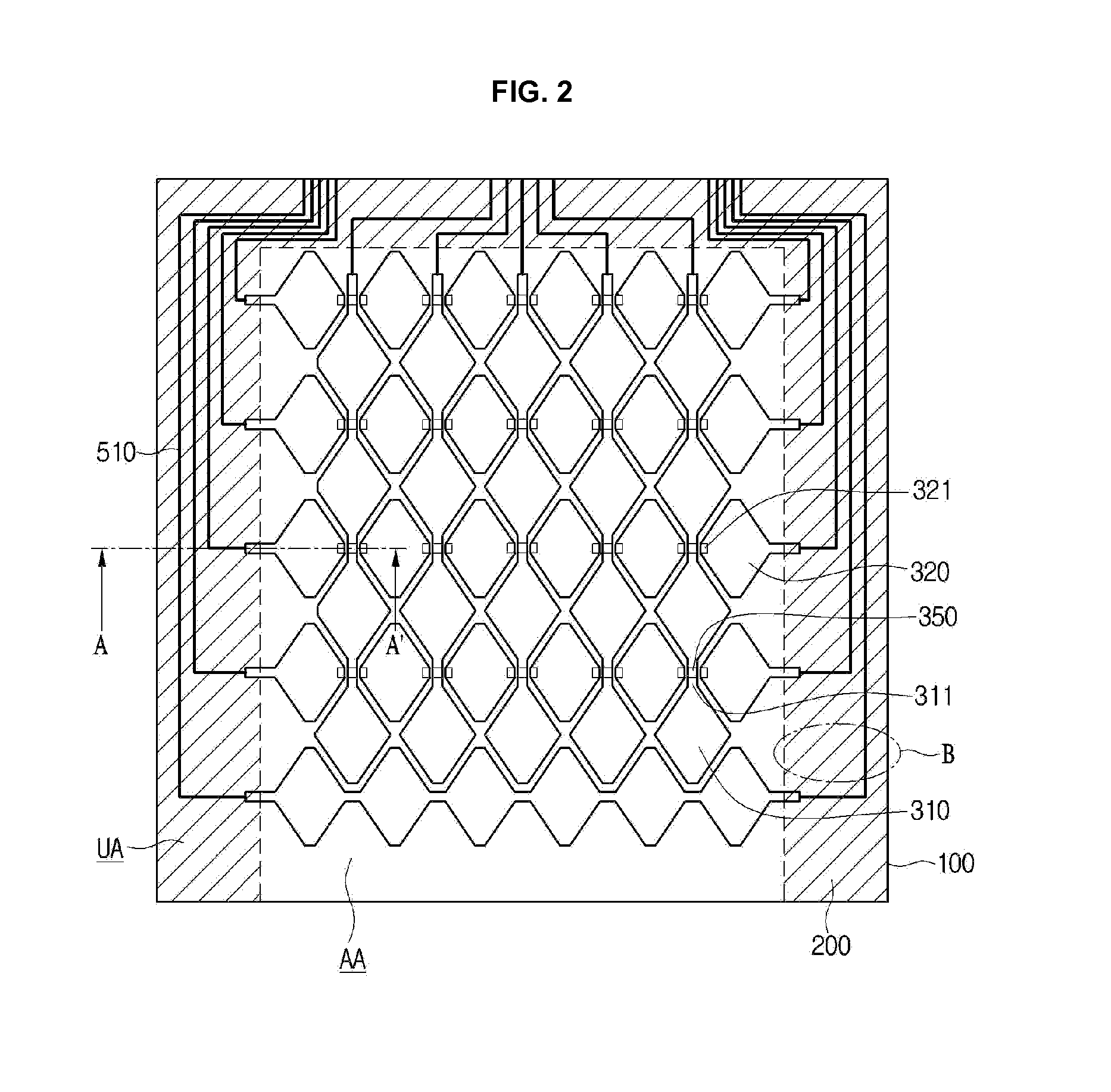
[0030]FIG. 1 is a perspective view showing a touch panel according to the embodiment. FIG. 2 is a plan view showing the touch panel according to the embodiment. FIG. 3 is an enlarged view of an area B shown in FIG. 2. FIG. 4 is a sectional view taken along line A-A′ of FIG. 2. FIG. 5 is a sectional view taken along line A-A′ of FIG. 2. A touch panel according to the embodiment may include a cover substrate 100, a printing layer 200, a sensing electrode 300, a wire electrode 400, and a printing circuit board 500.

[0031]The cover substrate 100 may support the printing layer 200, the sensing electrode 300, the wire electrode 400, and the printing circuit board 500. In other words, the cover substrate 100 may be a support substrate.

[0032]The cover substrate 100 may be flexible or rigid. For example, the cover substrate 100 may include glass or plastic. In detail, the cover substrate 100 may include chemically tempered / semi-tempered glass, such as soda lime glass or aluminosilicate glass,...


PUM

PropertyMeasurementUnit
thicknessaaaaaaaaaa
thickness T1aaaaaaaaaa

Abstract

Provided is a touch panel including a cover substrate including an active area and an unactive area, and a printing layer on the unactive area. The printing layer has surface roughness in a range of 0.4 μm to 0.6 μm. The printing layer has straightness in a range of ±0.1 μm to ±10 μm.

Description

CROSS-REFERENCE TO RELATED APPLICATIONS[0001]This application claims priority under 35 U.S.C. §119 to Korean Application No. 10-2014-0077392 filed Jun. 24, 2014, No. 10-2014-0079214 filed Jun. 26, 2014, No. 10-2014-0081681 filed Jul. 1, 2014 and No. 10-2014-0081682 filed Jul. 1, 2014, whose entire disclosures are hereby incorporated by reference.BACKGROUND[0002]1. Field[0003]This disclosure relates to a touch panel.[0004]2. Background[0005]Recently, a touch panel, which performs an input function through the touch to an image displayed on a display device by an input device, such as a stylus pen or a finger, has been applied to various electronic appliances. The touch panel includes a cover substrate having an active area to sense a position and an unactive area provided at a peripheral portion of the active area. A printing layer may be provided in the unactive area. The printing layer may be printed with a material representing a predetermined color so that a wire electrode and a ...

Claims


Application Information

Patent Timeline
Patent Type & Authority Applications(United States)
IPC IPC(8): H05K1/02G06F3/0354G06F3/047G06F3/041G06F3/044
CPCH05K1/0274H05K1/0271G06F2203/04809G06F2203/04808G06F2203/04112H05K2201/0145G06F2203/04107G06F2203/04101G06F3/047G06F3/0412G06F3/03545G06F2203/04111G06F3/044G06F3/04164G06F3/0443G06F3/0446
Inventor KIM, SOO KEUNRYU, JI CHANGHER, JAE HAK
Owner LG INNOTEK CO LTD
Why Eureka
Try Eureka