Flip chip bonder and flip chip bonding method

a technology of flip chip and bonding method, which is applied in the direction of soldering apparatus, manufacturing tools,auxillary welding devices, etc., can solve the problems of difficult liquid resin injection, time-consuming and laborious, and the gap between the chip and the circuit board has become increasingly small, so as to reduce the bonding time and reduce the bonding quality

Active Publication Date: 2015-12-31
SHINKAWA CO LTD
View PDF25 Cites 8 Cited by
  • Summary
  • Abstract
  • Description
  • Claims
  • Application Information

AI Technical Summary

Benefits of technology

[0019]The present invention provides an effect of providing a flip chip

Problems solved by technology

However, using an underfill material has a problem that filling of a liquid resin requires times, as well as a problem that it has become difficult to inject a liquid resin under a present circumstance that a gap between a chip and a circuit board has become increasingly smaller.
Upon completion of the bonding, the bonding tool is heated as high as about 300° C. Therefore, if the bonding tool receives a chip coming next from the holding membe

Method used


Image

  • Flip chip bonder and flip chip bonding method
  • Flip chip bonder and flip chip bonding method
  • Flip chip bonder and flip chip bonding method

Examples


Embodiment Construction

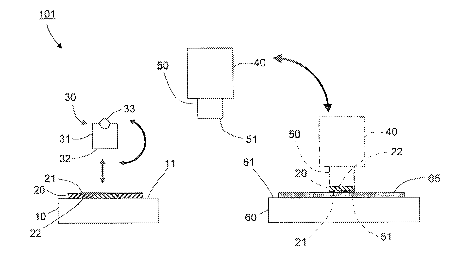
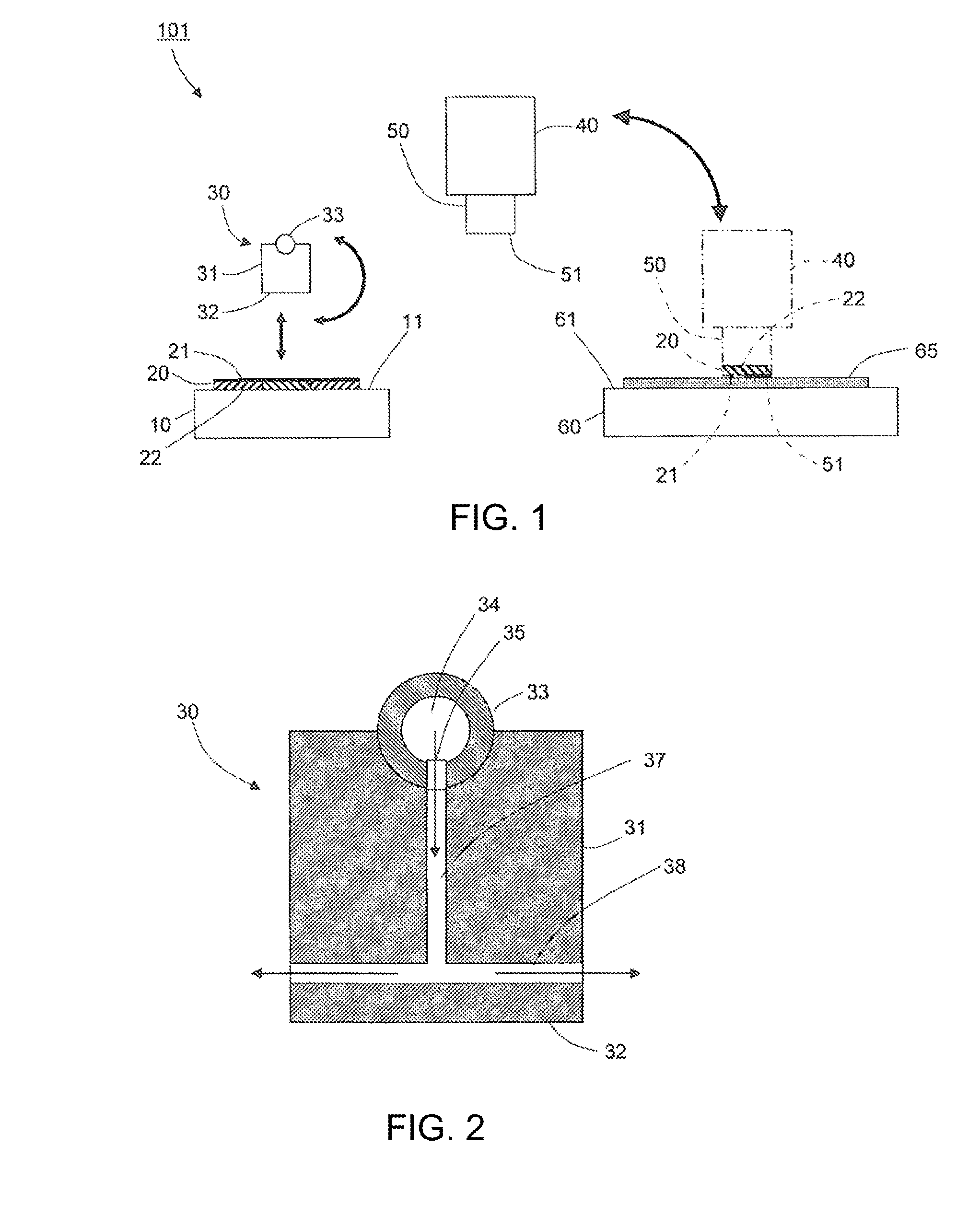
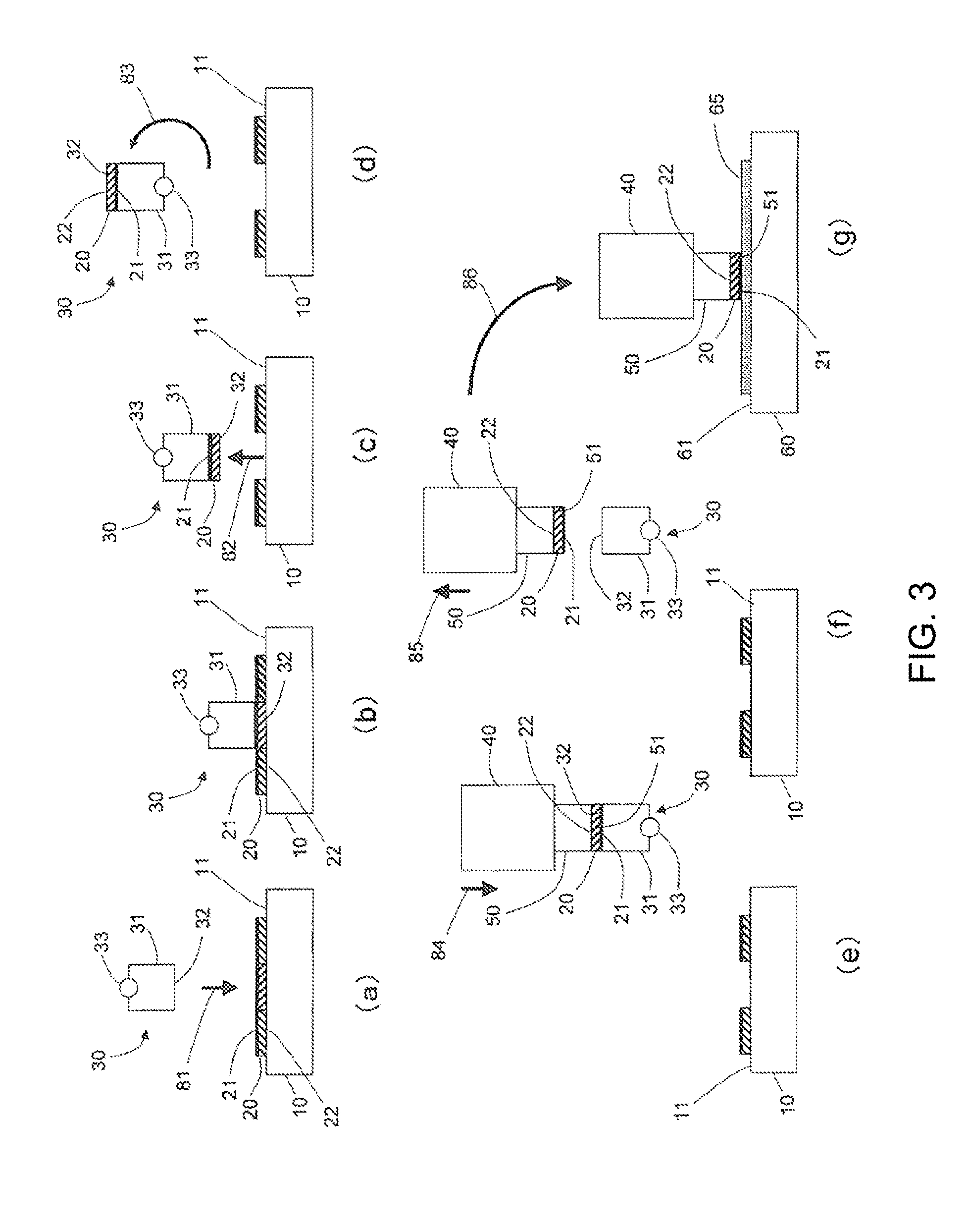
[0041]Hereinafter, embodiments according to the present invention will be described with reference to the drawings. As illustrated in FIG. 1, a flip chip bonder 101 according to one embodiment picks a chip 20 having a surface 22 to which a non-conductive film (NCF) 21 is applied and flips the chip, and then mounts (bonds) the chip onto a circuit board 65 on a bonding stage 60. The flip chip bonder 101 according to this embodiment includes: a pick-up stage 10 configured to hold the chip 20 on an upper surface 11 thereof; a pickup flipping collet 30 as a flip mechanism configured to picks the chip 20 up from the upper surface 11 of the pick-up stage 10 by suctioning, and flips the picked chip 20; and a bonding tool 50 configured to receive the flipped chip 20 from the pickup flipping collet 30 to bond the received chip 20 to the circuit board 65 fixed by suctioning on the bonding stage 60.

[0042]The pickup flipping collet 30 includes a collet main body 31 as a holding member having a s...


PUM

PropertyMeasurementUnit
Temperatureaaaaaaaaaa
Heataaaaaaaaaa
Heat capacityaaaaaaaaaa

Abstract

Provided is a flip chip bonder including: a pickup flipping collet configured to flip a chip; and a bonding tool configured to receive the chip flipped with the pickup flipping collet from the pickup flipping collet and to bond the received chip to a circuit board. The pickup flipping collet includes a cooling channel through which cooling air flows to cool the pickup flipping collet. Thus, bonding time can be reduced without lowering bonding quality.

Description

CROSS REFERENCE TO RELATED APPLICATIONS[0001]This application is a Continuation of PCT International Application No. PCT / JP2013 / 075478 filed on Sep. 20, 2013, which claims priority under 35 U.S.C §119(a) to Patent Application No. 2013-049541 filed in Japan on Mar. 12, 2013, all of which are hereby expressly incorporated by reference into the present application.TECHNICAL FIELD[0002]The present invention relates to a structure of a flip chip bonder and a flip chip bonding method using a flip chip bonder.BACKGROUND ART[0003]Flip chip bonding in which bump electrodes also called bumps are formed on a chip and the chip is directly connected to a circuit board has become widely employed as a method of mounting a chip on a circuit board. The flip chip bonding is a method for joining a chip and a circuit board by forming a plurality of bumps (bump electrodes) made of a material such as solder on a circuit side of the chip, and heating and melting the bumps to join the bumps to a plurality ...

Claims


Application Information

Patent Timeline
IPC IPC(8): H01L23/00
CPCH01L2224/131H01L24/75H01L2224/2919H01L2224/32225H01L2224/73204H01L2224/9211H01L2224/16227H01L24/81H01L2224/8385H01L2224/8388H01L2224/83203H01L2224/81203H01L2224/75744H01L2224/75252H01L2224/83948B23K37/04B23K3/085H01L2924/3701H01L2224/81948H01L2224/16225H01L2224/75621H01L2224/7565H01L2224/75501H01L2224/75502H01L2224/73104H01L2224/75745H01L2224/81191H01L2224/81815H01L2224/83H01L2224/83191H01L2224/83862H01L2924/00012H01L2924/00014H01L2924/014H01L2224/81H01L2924/00H01L21/52H01L21/67H01L21/67005
Inventor SEYAMA, KOHEI
Owner SHINKAWA CO LTD
Why Eureka
Try Eureka