Method for preventing read-disturb errors, memory control circuit unit and memory storage apparatus
- Summary
- Abstract
- Description
- Claims
- Application Information
AI Technical Summary
Benefits of technology
Problems solved by technology
Method used
Image
Examples
first exemplary embodiment
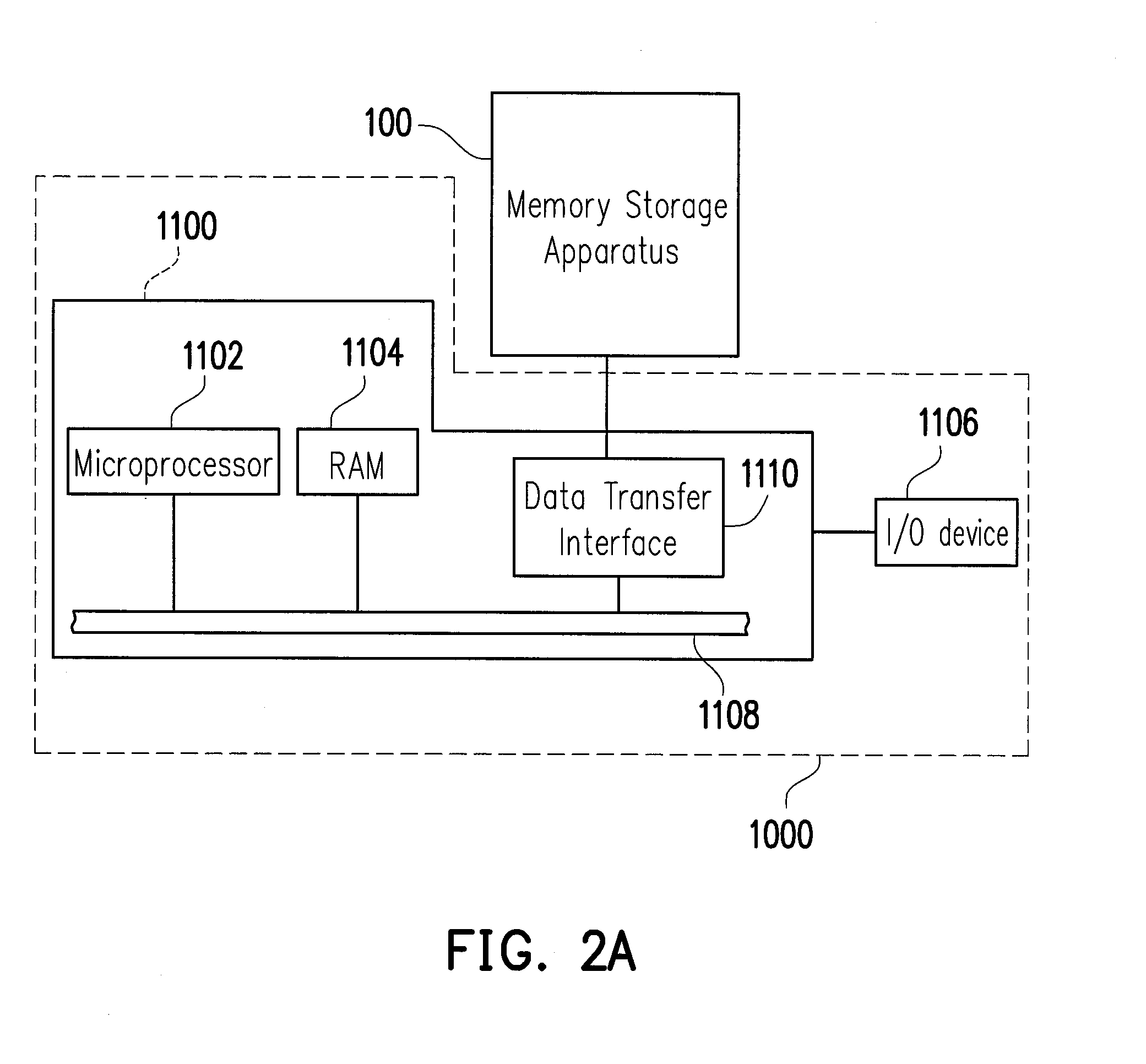
[0036]FIG. 2A is a schematic diagram illustrating a host system and a memory storage apparatus according to the first exemplary embodiment of the present invention. FIG. 2B is a schematic diagram illustrating a computer, an input / output device and a memory storage apparatus according to the first exemplary embodiment of the present invention. FIG. 2C is a schematic diagram illustrating the host system and the memory storage apparatus according to an example.
[0037]Referring to FIG. 2A, host system 1000 generally includes a computer 1100 and an I / O (input / output) device 1106. The computer 1100 may include a microprocessor 1102, a RAM (random access memory) 1104, a system bus 1108 and a data transmission interface 1110. The input / output device 1106 may include a mouse 1202, a keyboard 1204, a monitor 1206 and a printer 1208 as shown in FIG. 2B. It is to be understood that the devices as shown in FIG. 2B do not intend to limit the input / output device 1106, and the input / output device 11...
second exemplary embodiment
[0085]The structure of the memory storage apparatus of the second exemplary embodiment is similar to that of the first exemplary embodiment except that the memory control circuit unit (or memory management circuit) of the second exemplary embodiment uses random method to select physical erasing unit to execute the operation for preventing read-disturb errors. The reference numerals of the first exemplary embodiment are used to illustrate the difference from the second exemplary embodiment hereinafter.
[0086]In the present exemplary embodiment, the memory control circuit unit 104 may further include a randomly selected module circuit (not shown), particularly, the memory control circuit unit 104 (or memory management circuit 202) executes an operation of random function through the randomly selected module circuit to select the physical erasing unit to execute the operation for preventing read-disturb errors. For example, the memory control circuit unit 104 (or memory management circu...
third exemplary embodiment
[0090]The structure of the memory storage apparatus of the third exemplary embodiment is similar to that of the first exemplary embodiment and the second exemplary embodiment, which both select the physical erasing unit in a random manner to execute the operation for preventing read-disturb errors. The difference is that in the third exemplary embodiment, the method of preventing read-disturb errors randomly selects a logical address first and then maps to the corresponding physical erasing unit, and the selected logical addresses are tagged such that the physical erasing unit selected each time to execute the operation for preventing read-disturb errors will not be repeated. The reference numerals of the first exemplary embodiment are used to illustrate the difference of the third exemplary embodiment hereinafter.
[0091]In the present exemplary embodiment, memory control circuit unit further includes a randomly selected module circuit (not shown), particularly, the memory control ci...
PUM
 Abstract
Description
Claims
Application Information


