ESD protection circuit

Active Publication Date: 2016-10-20
SHANGHAI HUAHONG GRACE SEMICON MFG CORP
View PDF7 Cites 0 Cited by
  • Summary
  • Abstract
  • Description
  • Claims
  • Application Information

AI Technical Summary

Benefits of technology

[0018]The present invention is beneficial over the prior art designs majorly in that, an RC trigger circuit and a transmission gate are used for determination of ESD protection triggering, and a silicon-controlled rectifier for ESD current conductance, wherein the RC trigger circuit and the transmission gate allow improved trigger efficiency, and

Problems solved by technology

However, the improvements also lead to a significant disadvantage.
Deep submicron ICs are more vulnerable to electrostatic discharge (ESD) strikes which can cause failure of the circuits, leading to lower reliability of products in which such ICs are used.
This event may cause a very large current flowing through the IC chip in a very short period of time.
As an ESD pulse is typically a high-voltage, high-frequency signal, the discharge transistor 20 is required to be a bulky device wi

Method used


Image

  • ESD protection circuit
  • ESD protection circuit

Examples


Example

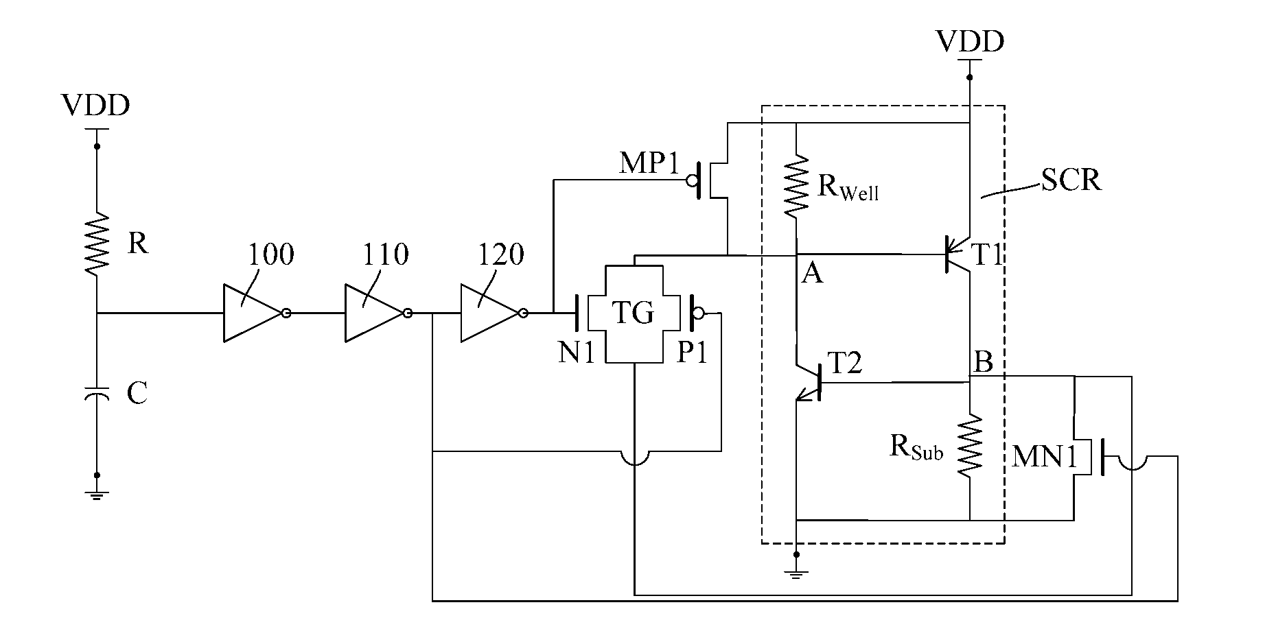
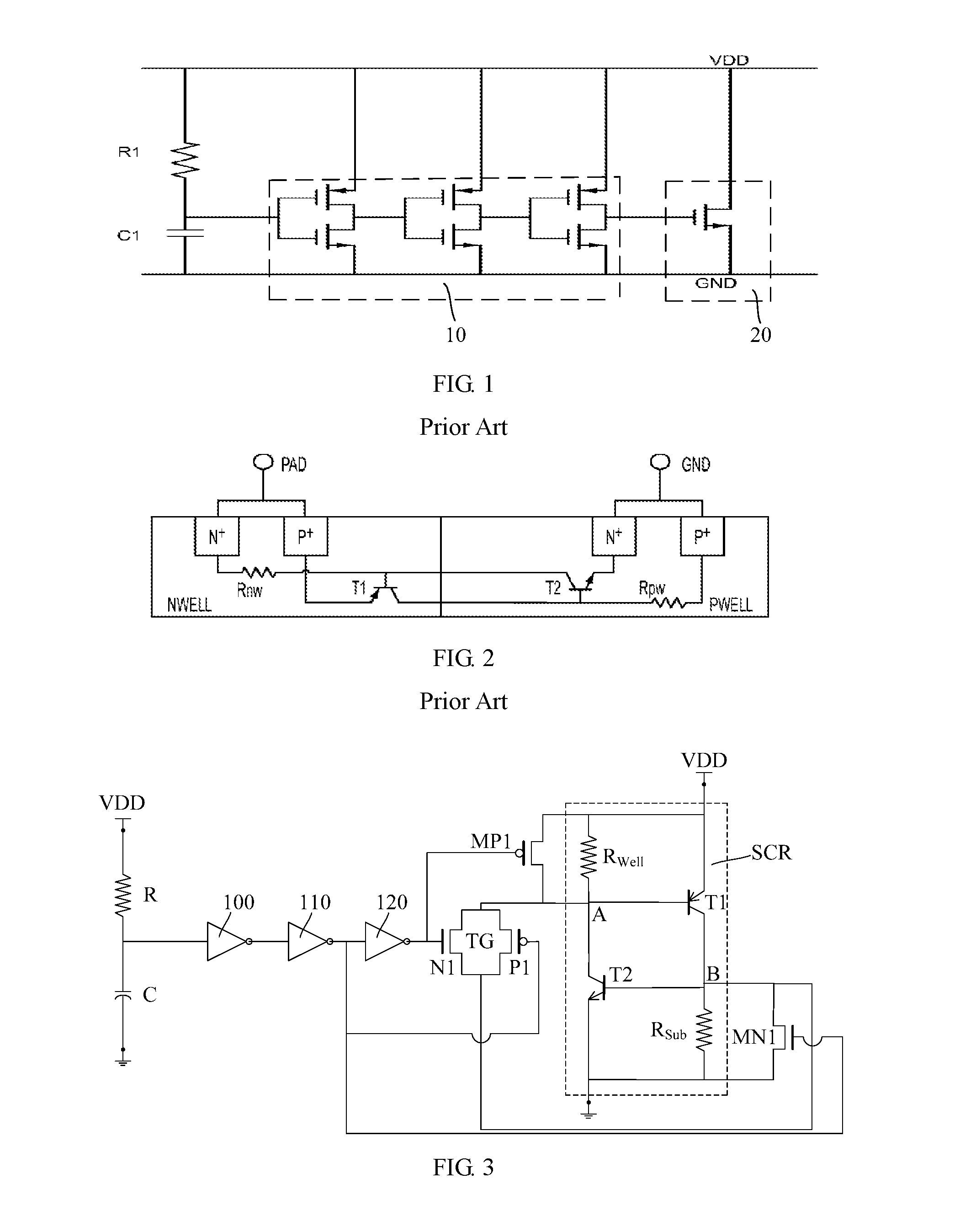
[0022]Electrostatic discharge (ESD) protection circuits according to the present invention will be described in greater detail in the following description which presents preferred embodiments of the invention, in conjunction with the accompanying drawings. It is to be appreciated that those of skill in the art can make changes in the invention disclosed herein while still obtaining the beneficial results thereof. Therefore, the following description shall be construed as widely known by those skilled in the art rather than as limiting the invention.

[0023]For simplicity and clarity of illustration, not all features of the specific embodiments are described. Additionally, description and details of well-known functions and structures are omitted to avoid unnecessarily obscuring the invention. The development of any specific embodiment of the present invention includes specific decisions made to achieve the developer's specific goals, such as compliance with system related and busines...


PUM


Abstract

An ESD protection circuit is disclosed, in which an RC trigger circuit and a transmission gate are used for determination of ESD protection triggering, and a silicon-controlled rectifier for ESD current conductance. The RC trigger circuit and the transmission gate allow improved trigger efficiency. In addition, the silicon-controlled rectifier incorporates first and second resistors, which can be implemented to have very low resistance values and are therefore able to effectively prevent the occurrence of latch-up during normal operation, as well as pull-up and pull-down transistors which can make an additional contribution to latch-up inhibition when turned on.

Description

CROSS-REFERENCES TO RELATED APPLICATIONS[0001]This application claims the priority of Chinese patent application number 201510185684.1, filed on Apr. 17, 2015, the entire contents of which are incorporated herein by reference.TECHNICAL FIELD[0002]The present invention relates to the field of integrated circuit (IC) design and manufacture and, more particularly, to electrostatic discharge (ESD) protection circuits.BACKGROUND[0003]With the integrated circuit (IC) fabrication technology developing to a stage where the device feature sizes reach deep-submicron dimensions, all circuit MOS devices are employed as lightly-doped drain (LDD) structures, and the silicide process has been widely used in the diffusion layers of such MOS devices. Meanwhile, in order to reduce the series resistance due to diffusion in gate polysilicon, synthesis of polycrystalline compounds is also employed. These fabrication process improvements can result in significant increases in IC operation speed and integ...

Claims


Application Information

Patent Timeline
IPC IPC(8): H02H9/04
CPCH02H9/046
Inventor LV, BIN
Owner SHANGHAI HUAHONG GRACE SEMICON MFG CORP
Why Eureka
Try Eureka