
Pixel, pixel driving method, and display device comprising the pixel

a driving method and pixel technology, applied in the field of pixels, can solve the problems of shortened lifespan, increased power consumption, and insufficient improvement of sheet resistance at the middle portion of the screen, and achieve the effect of reducing the sheet resistance of the cathode electrode and lowering the driving voltag

Active Publication Date: 2016-01-14
SAMSUNG DISPLAY CO LTD
View PDF6 Cites 32 Cited by
  • Summary
  • Abstract
  • Description
  • Claims
  • Application Information

AI Technical Summary

Benefits of technology

The present invention provides a method for reducing the resistance of a display device's cathode electrode and lowering the voltage required for driving. This is achieved by utilizing a pixel sensing line, which improves operational stability. The technical effects of this invention include improved driving stability, reduced power consumption, and improved user experience.

Problems solved by technology

However, the position of the the auxiliary electrode is limited to a non-emission region, and thus the sheet resistance is not sufficiently improved at a middle portion on a screen.
Accordingly, a driving voltage needs to be increased to compensate for a voltage drop, which causes power consumption to be increased and lifespan to be shortened.

Method used


Image

  • Pixel, pixel driving method, and display device comprising the pixel
  • Pixel, pixel driving method, and display device comprising the pixel
  • Pixel, pixel driving method, and display device comprising the pixel

Examples


Embodiment Construction

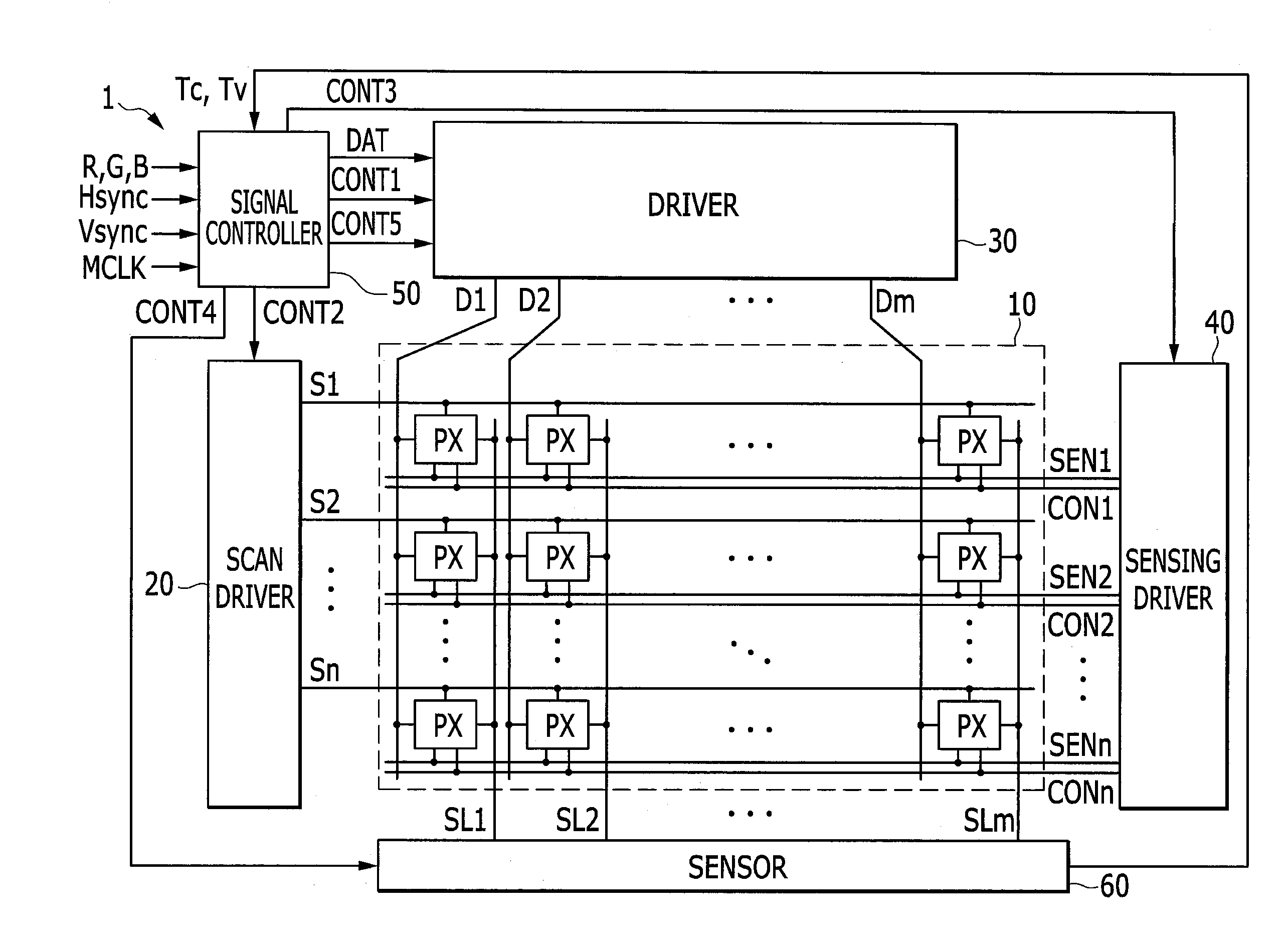
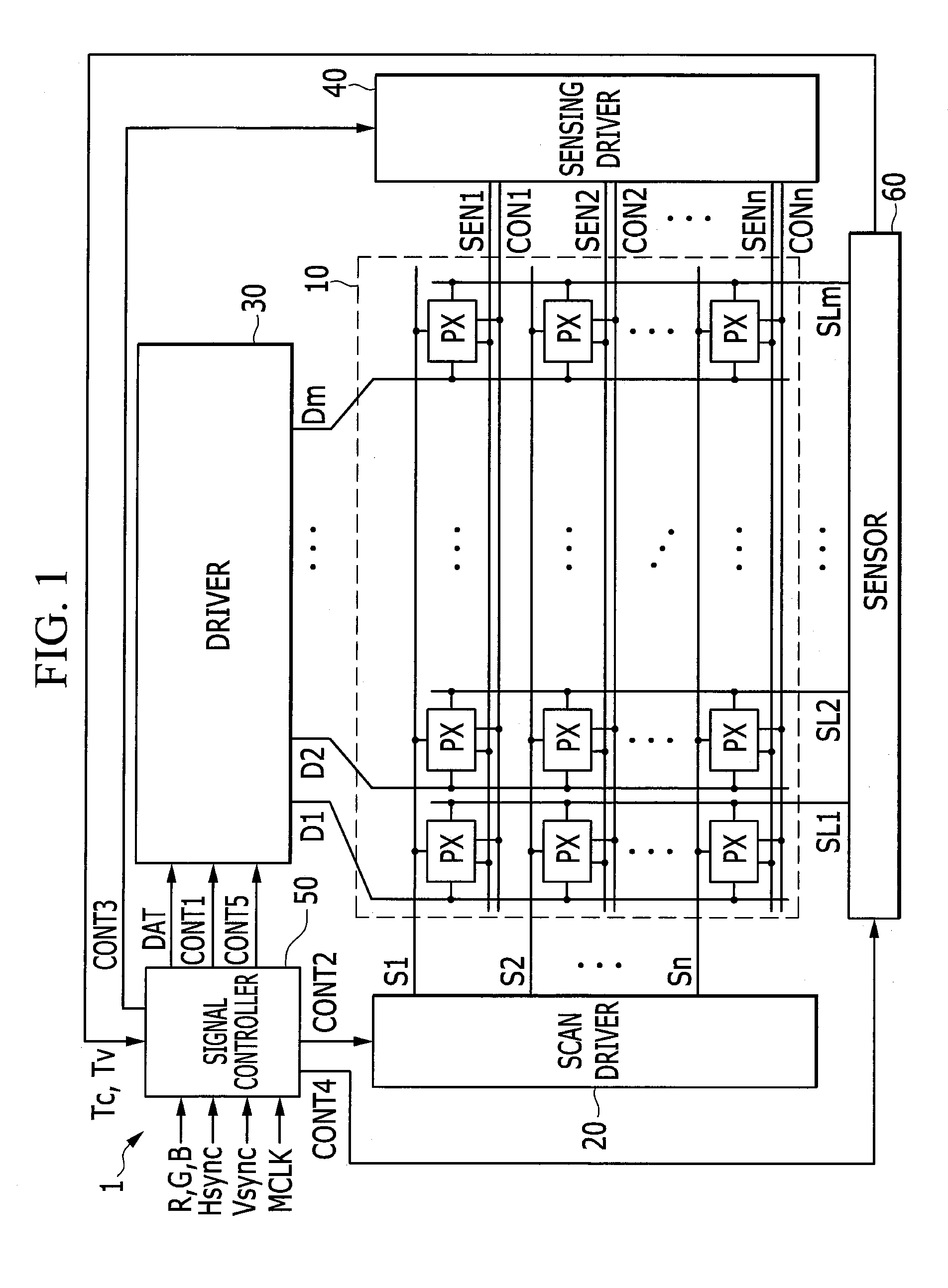
[0033]Hereinafter, exemplary embodiments of the present invention will be described in detail with reference to the accompanying drawings. Herein, the same or similar components will be denoted by the same key numerals, and overlapping descriptions thereof may be omitted. The terms “module” and “unit” are used for describing components in the following description to make the specification easier to understand. Therefore, these terms do not have meanings or roles that distinguish components from each other by themselves. In describing exemplary embodiments of the present invention, when it is determined that a detailed description of well-known components or art associated with embodiments of the present invention may obscure the features of embodiments of the present invention, the detailed description of the components or art will be omitted. The accompanying drawings are provided only in order to allow exemplary embodiments disclosed herein to be easily understood and are not to ...


PUM


Abstract

An exemplary embodiment of the present invention provides a pixel including: a pixel including: a switching transistor configured to perform a switching operation according to a scan signal, the switching transistor including a first terminal that is coupled to a data line and a second transistor; a driving transistor configured to control a driving current according to a data signal that is transferred when the switching transistor is turned on, the driving transistor including a gate that is coupled to the second terminal of the switching transistor; a light-emitting element comprising a cathode and configured to emit light according to the driving current; and a contact transistor configured to perform a switching operation according to a sensing control line, the contact transistor including a first terminal coupled to the cathode electrode of the light-emitting element and a second terminal that is coupled to a sensing line to which a current of the driving transistor is applied.

Description

CROSS-REFERENCE TO RELATED APPLICATION[0001]This application claims priority to and the benefit of Korean Patent Application No. 10-2014-0086107 filed in the Korean Intellectual Property Office on Jul. 9, 2014, the entire contents of which are incorporated herein by reference.BACKGROUND[0002]1. Field[0003]Embodiments of the present invention relate to a pixel, a pixel driving method, and a display device including the pixel.[0004]2. Description of the Related Art[0005]An organic light emitting display has a display area formed by arranging a plurality of pixels PX on a substrate in a matrix form, and performs display by connecting each pixel to a scan line and a data line and selectively applying a data signal to the pixel.[0006]The organic light emitting display is a flat panel display that displays an image by using organic light emitting diodes (OLEDs) which generate light by re-combining electrons and holes, and has been in the spotlight because it has a quick response speed, lo...

Claims


Application Information

Patent Timeline
Patent Type & Authority Applications(United States)
IPC IPC(8): G09G3/32G09G5/18
CPCG09G5/18G09G2300/0426G09G3/3208G09G3/3233G09G2300/043G09G2300/0819G09G2320/0223G09G2320/0295G09G2320/043G09G2320/045
Inventor KIM, SU, WEON
Owner SAMSUNG DISPLAY CO LTD
Learn More