
Organic light emitting display devices and methods of manufacturing organic light emitting display devices

Active Publication Date: 2016-01-14
SAMSUNG DISPLAY CO LTD
View PDF29 Cites 10 Cited by
  • Summary
  • Abstract
  • Description
  • Claims
  • Application Information

AI Technical Summary

Benefits of technology

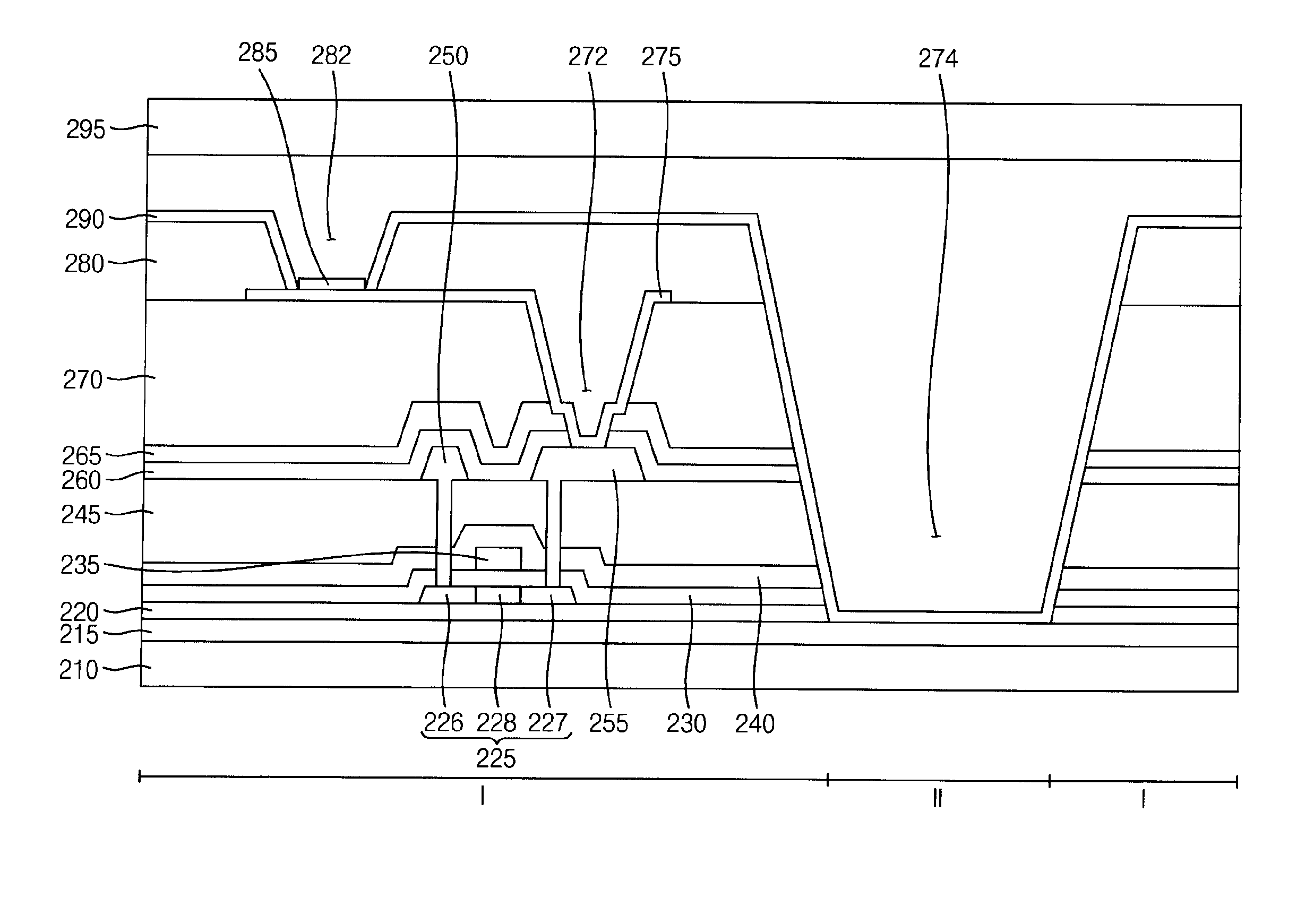
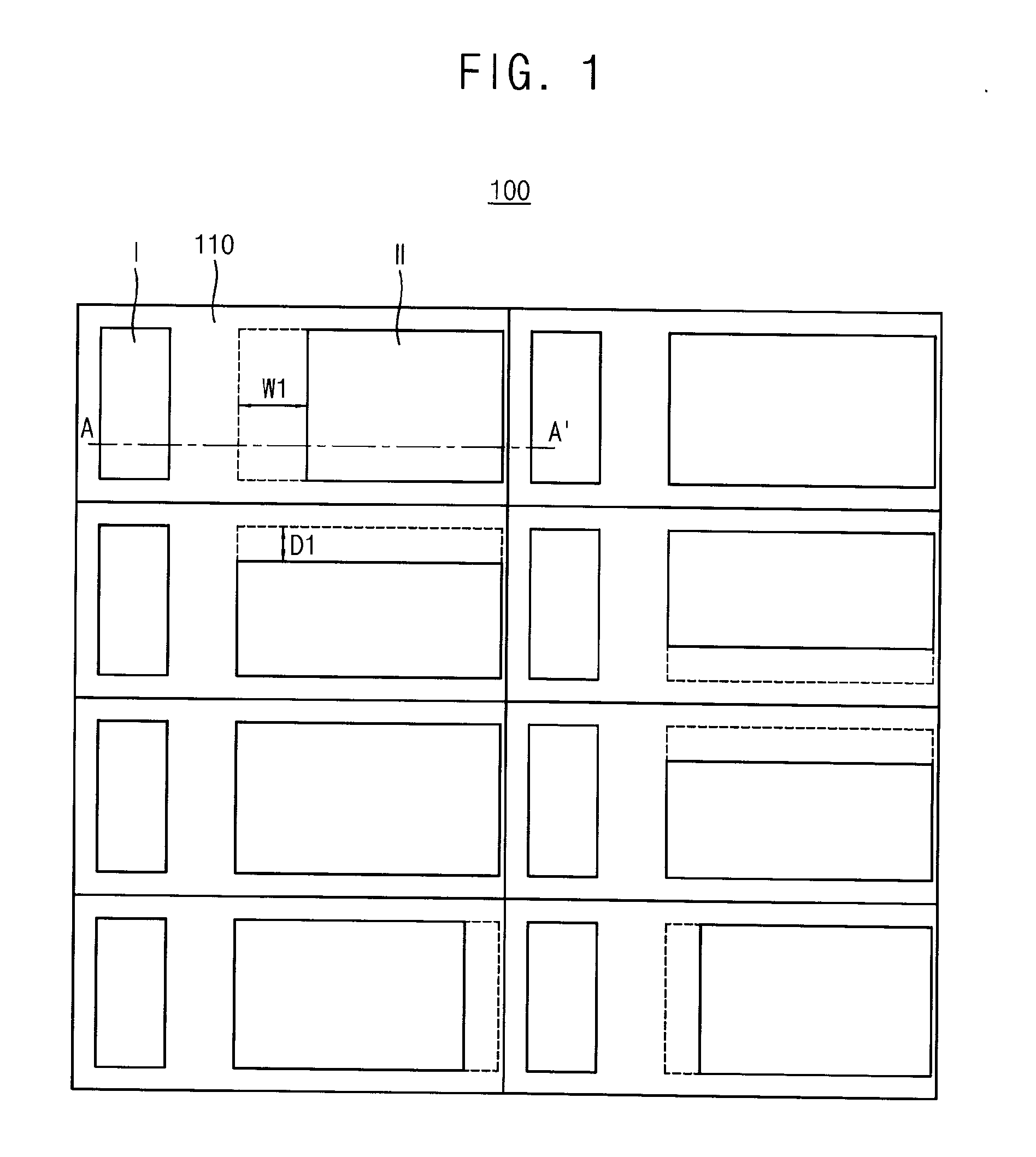
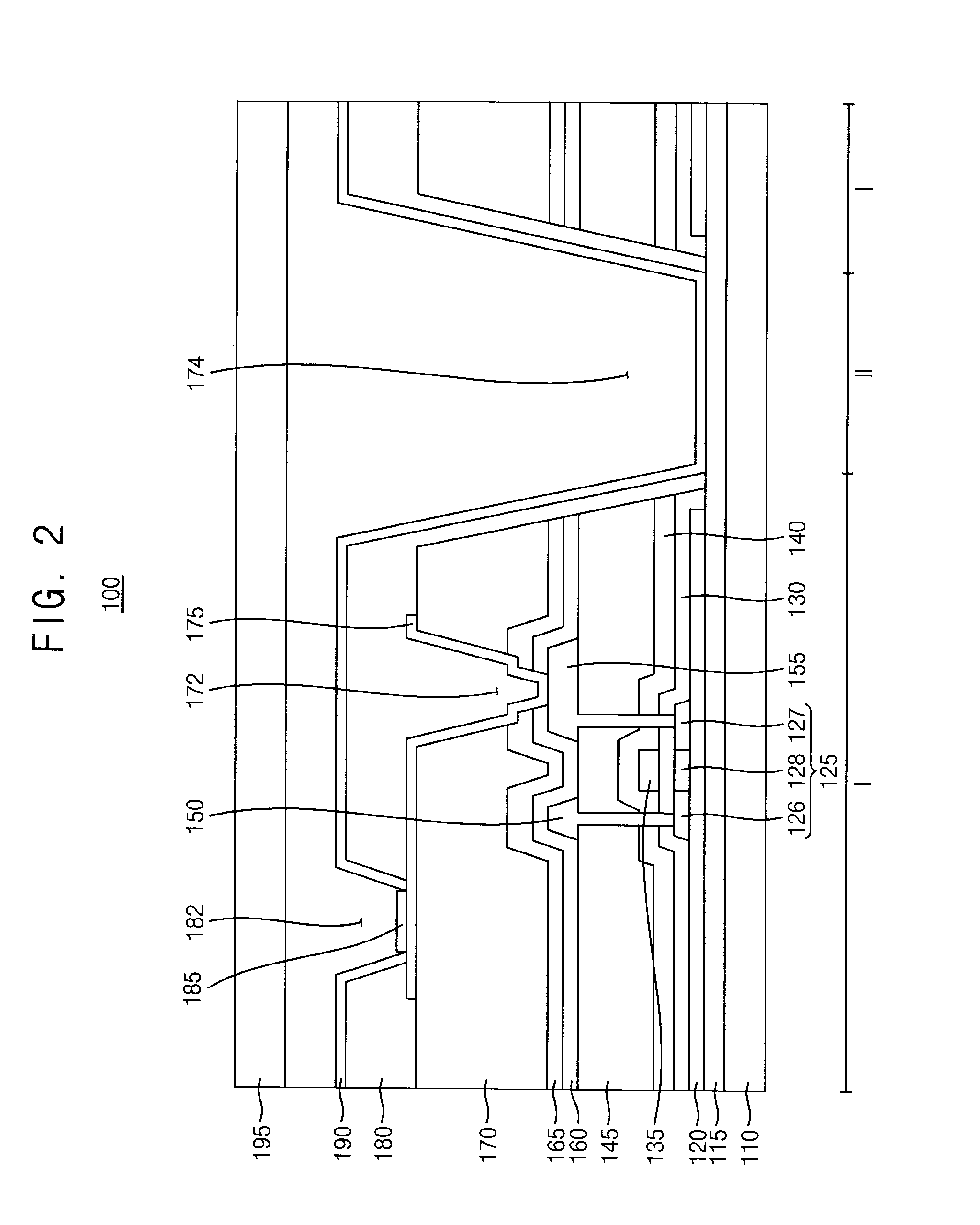
The patent describes an organic light emitting display device that includes transparent regions arranged in an asymmetrical configuration to prevent image distortion and improve the quality of displayed images. When the device is in an off state, the transparent regions are designed to reduce or eliminate diffraction interference, while when the device is in an on state, the transparent regions are designed to enhance the image quality. A pixel defining layer with openings partially exposing the transparent regions may be used to at least partially define the shapes of adjacent transparent regions, and the adjacent transparent regions may have different surface areas to further suppress diffraction interference. This asymmetrical configuration of adjacent transparent regions helps prevent image distortion and improves the quality of images displayed on the organic light emitting display device.

Problems solved by technology

The multiple slits may cause diffraction interference of a light passing therethrough, so that the image of the object viewed through the conventional transparent organic light emitting display device may be distorted, while the conventional transparent organic light emitting display device is in the OFF state.
Such image distortion may reduce the quality of images displayed in the pixel region, while the conventional transparent organic light emitting display device is in the ON state.

Method used


Image

  • Organic light emitting display devices and methods of manufacturing organic light emitting display devices
  • Organic light emitting display devices and methods of manufacturing organic light emitting display devices
  • Organic light emitting display devices and methods of manufacturing organic light emitting display devices

Examples


Embodiment Construction

[0022]Hereinafter, organic light emitting display devices and methods of manufacturing the organic light emitting display devices in accordance with exemplary embodiments will be explained in detail with reference to the accompanying drawings.

[0023]It will be understood that when an element or layer is referred to as being “on” or “connected to” another element or layer, it can be directly on or directly connected to the other element or layer, or intervening elements or layers may be present. In contrast, when an element is referred to as being “directly on” or “directly connected to” another element or layer, there are no intervening elements or layers present. It will be understood that for the purposes of this disclosure, “at least one of X, Y, and Z” can be construed as X only, Y only, Z only, or any combination of two or more items X, Y, and Z (e.g., XYZ, XYY, YZ, ZZ).

[0024]FIG. 1 is a plan view illustrating an organic light emitting display device in accordance with exemplary...


PUM


Abstract

An organic light emitting display device includes a substrate including a plurality of pixel regions and a plurality of transparent regions, thin film transistors disposed in the pixel regions, an insulation layer disposed on the thin film transistors, first electrodes electrically contacting the thin film transistors, a pixel defining layer including a black material disposed on the first electrodes, organic light emitting structures disposed on the pixel defining layer, and a second electrode disposed on the organic light emitting structures. The pixel defining layer may define an asymmetrical configuration of adjacent transparent regions disposed on opposing sides of corresponding pixel regions.

Description

CROSS-REFERENCE TO RELATED APPLICATION[0001]This application claims priority from and the benefit of Korean patent Application No. 10-2014-0088223, filed on Jul. 14, 2014, which is hereby incorporated by reference for all purposes as if fully set forth herein.BACKGROUND[0002]1. Field[0003]Exemplary embodiments of the present disclosure relate to organic light emitting display devices and methods of manufacturing organic light emitting display devices. More particularly, exemplary embodiments of the disclosure relate to organic light emitting display devices including a plurality of transparent regions arranged in an asymmetrical configuration and methods of manufacturing the organic light emitting display devices.[0004]2. Discussion of the Background[0005]Recently, a transparent organic light emitting display device has been developed as a next-generation display devices. The transparent organic light emitting display device may include a transparent region and a pixel region. In th...

Claims


Application Information

Patent Timeline
IPC IPC(8): H01L27/32H01L51/56
CPCH01L27/3272H01L51/56H01L27/3246H10K59/121H10K59/126H10K59/122
Inventor AHN, KI-WANPARK, SANG-HOJANG, YONG-JAE
Owner SAMSUNG DISPLAY CO LTD
Learn More