Unlock instant, AI-driven research and patent intelligence for your innovation.

3D stacked memory array and method for determining threshold voltages of string selection transistors

Active Publication Date: 2016-01-21
SEOUL NAT UNIV R&DB FOUND
View PDF1 Cites 1 Cited by
  • Summary
  • Abstract
  • Description
  • Claims
  • Application Information

AI Technical Summary

Benefits of technology

The present invention provides a way to make 3D memory arrays by using a method called LSMP to determine the threshold voltage of string selection transistors. This method allows for the selection of layers without being limited by the number of available threshold voltage states or SSLs (semiconductor etching process). By using this method, memory can be made more efficiently by reducing the number of SSLs needed, and layers can be selected without limitation based on the aspect ratio of the etching process.

Problems solved by technology

Recently, there has been difficulty in improving the degree of integrity under 20 nm due to limitation of the photolithography technology.
However, because the LASER structure is consisted of sting selection transistors formed at locations crossed between each SSL and an active line (each layer of bit lines) and simply divided into initialized transistors and not, there have been some limitations in improving the degree of integrity by minimizing the number of SSLs for a layer selection.
However, if n is an odd number, there has been a problem that one of SSLs is not paired.

Method used


Image

  • 3D stacked memory array and method for determining threshold voltages of string selection transistors
  • 3D stacked memory array and method for determining threshold voltages of string selection transistors
  • 3D stacked memory array and method for determining threshold voltages of string selection transistors

Examples


Embodiment Construction

[0039]Detailed descriptions of preferred embodiments of the present invention are provided below with accompanying drawings.

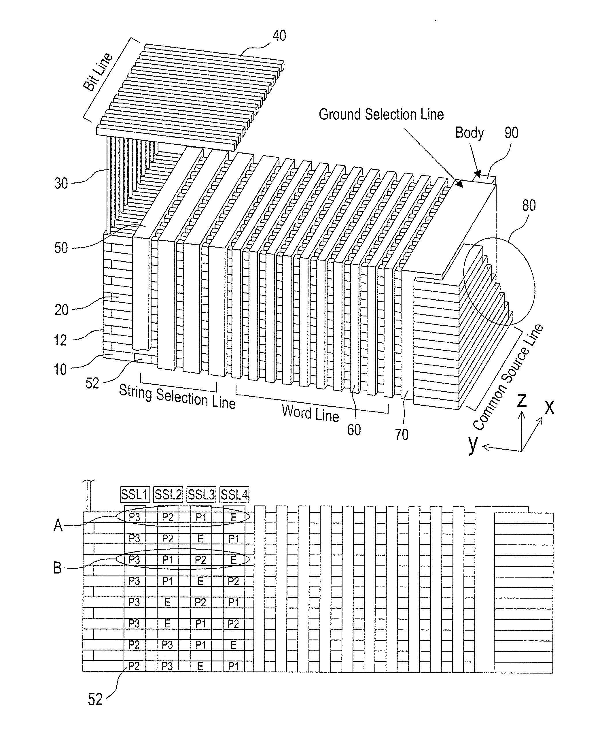
[0040]First, a 3D stacked memory array according to an embodiment of the present invention is comprising: as drawn in FIG. 1A, a plurality of active lines (for example, lines connected to a bit line 40) formed at regular intervals in a first horizontal direction (for example, in an x-axis direction) with a plurality of semiconductor layers 10 vertically stacked having insulating films 20 between upper and lower layers on a substrate (not shown); a plurality of word lines 60 formed at regular intervals in second horizontal direction (for example, in a y-axis direction) to be vertically aligned to each of the active lines and to pass by the plurality of semiconductor layers 10 with insulating layers (not shown) including a charge storage layer between each of the word lines and the semiconductor layers; and a plurality of string selection lines 50 formed at regul...


PUM


Abstract

This invention provides 3D stacked memory arrays and methods for determining threshold voltages of string selection transistors by LSMP (layer selection by multi-level permutation) for enabling to select layers regardless of the number or as many as possible by the limited numbers of threshold voltage states and SSLs. Thus, this invention enables to maximize the degree of integrity of memory by minimizing the number of SSLs and to select layers with no limitation of the number by considering a recent aspect ratio of the semiconductor etching process.

Description

CROSS REFERENCE TO RELATED APPLICATION[0001]This application claims priority to Korean Patent Application No. 10-2014-0089558, filed on Jul. 16, 2014, under 35 U.S.C. 119, the entire contents of which are hereby incorporated by reference.BACKGROUND[0002]1. Field of the Invention[0003]The present invention relates to a three-dimensional (3D) stacked memory array, and more particularly to a 3D stacked memory array enabling to select layers as a general method or to improve the degree of integrity of a memory by selecting layers as many as possible under the limited number of threshold voltage states of string selection transistors and the limited number of string selection lines (SSLs), and to a method for determining threshold voltages of string selection transistors of the same array.[0004]2. Description of the Related Art[0005]Recently, there has been difficulty in improving the degree of integrity under 20 nm due to limitation of the photolithography technology. So, various memory...

Claims


Application Information

Patent Timeline
IPC IPC(8): G11C16/34G11C16/04H01L27/115
CPCG11C16/34H01L27/1157G11C16/0466G11C16/0483H01L27/11582G11C8/12G11C8/14G11C11/5621G11C11/5628H10B43/20H10B43/35G11C2213/71H10B43/27
Inventor PARK, BYUNG-GOOKLEE, SANG-HO
Owner SEOUL NAT UNIV R&DB FOUND
Features
  • R&D
  • Intellectual Property
  • Life Sciences
  • Materials
  • Tech Scout
  • Unparalleled Data Quality
  • Higher Quality Content
  • 60% Fewer Hallucinations
Learn More