Thin film transistor and display device using the same

Active Publication Date: 2016-02-04
LG DISPLAY CO LTD
View PDF3 Cites 4 Cited by
  • Summary
  • Abstract
  • Description
  • Claims
  • Application Information

AI Technical Summary

Benefits of technology

[0010]An advantage of the present invention is to provide a display panel including an oxide thin film transistor, in which the source electrode and the drain electrode of the TFT are configured to suppress the threshold voltage shift of the TFT.
[0011]Additional advantages and features of the invention will be set forth in part in the description which follows and in part will become apparent to those having ordinary skill in the art upon examination of the following or may be learned from practice of the invention. These other advantages of the invention may be realized and attained by the structure particularly pointed out in the written description and claims hereof as well as the appended drawings.
[0012]Accordingly, the display panel includes an oxide TFT in which one of the source electrode and drain electrode of the oxide TFT extends more onto the etch stopper layer towards the other electrode. That is, on the etch stopper layer at the central portion of the active layer, the length in which the drain electrode is extended toward the source electrode is greater than the length in which the source electrode is extended toward the drain electrode.
[0013]More specifically, in an embodiment, a thin film transistor comprises an oxide semiconductor active layer, a gate electrode, a first electrode in contact with a source region of the active layer and a second electrode in contact with a drain region of the active layer. A gate insulating film is provided between the gate electrode and the active layer. Further, an etch stopper layer is provided on the active lay

Problems solved by technology

The misalignment during the fabrication of the TFT may cause a short channel phenomenon, in which the channel length of the TFT becomes short due to a drain bias.
As the

Method used


Image

  • Thin film transistor and display device using the same
  • Thin film transistor and display device using the same
  • Thin film transistor and display device using the same

Examples


Embodiment Construction

[0026]Hereinafter, the present invention will be described in detail with reference to the accompanying drawings.

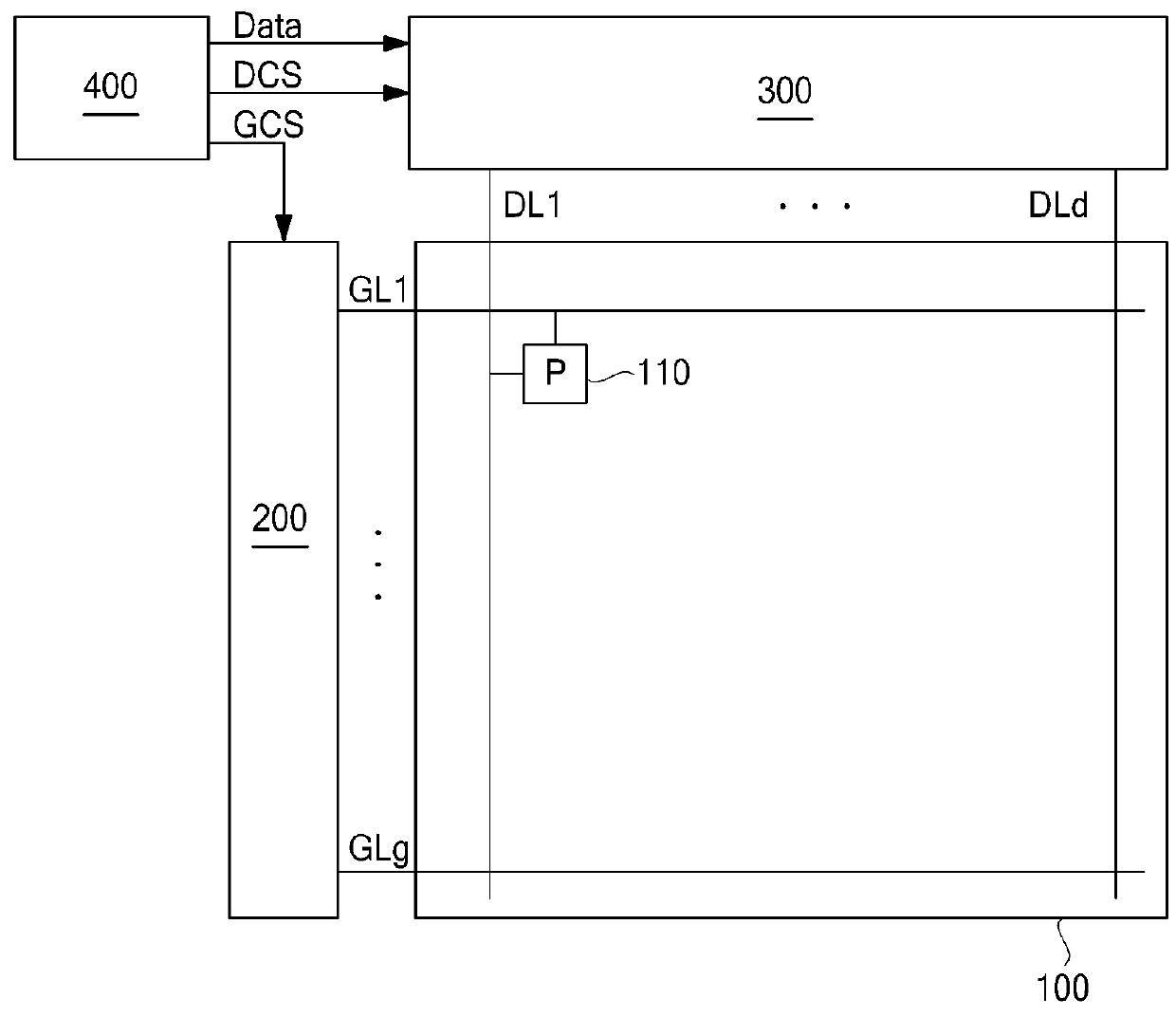
[0027]FIG. 1 is a schematic illustration of a display device according to an embodiment of the present invention.

[0028]The display device according to an embodiment of the present invention, as shown in FIG. 1, includes a panel 100 provided with a pixel 110 formed per crossing area of gate lines GL1 to GLg and data lines DL1 to DLd, a gate driver 200 for sequentially supplying scan pulses to the gate lines GL1 to GLg formed in the panel 100, a data driver 300 for supplying a data voltage to the data lines DL1 to DLd formed in the panel 100, and a timing controller 400 for controlling functions of the gate driver 200 and the data driver 300.

[0029]The panel 100 may be, for example, a liquid crystal display panel. A plurality of data lines DL1 to DLd and a plurality of gate lines GL1 to GLg are provided on a lower substrate (TFT substrate) of the panel 100. An oxide thin fil...


PUM


Abstract

A display panel including an oxide thin film transistor is disclosed. In the oxide thin film transistor, a part of the active layer between a source region and a drain region is covered with an etch stopper layer, and the etch stopper layer is partially covered by the first electrode and the second electrode of the oxide thin film transistor. The length in which the etch stopper layer is overlapped by the second electrode is greater than the length in which the etch stopper layer is overlapped by the first electrode to suppress threshold voltage shift in the oxide thin film transistor.

Description

CROSS REFERENCE TO RELATED APPLICATIONS[0001]This application claims the benefit of Korean Patent Application No. 10-2014-0098657 filed on Jul. 31, 2014, which is hereby incorporated by reference for all purposes as if fully set forth herein.BACKGROUND OF THE INVENTION[0002]1. Field of the Invention[0003]The present invention relates to a display device. More particularly, the present invention relates to a display device including an oxide thin film transistor.[0004]2. Discussion of the Related Art[0005]Flat panel displays (FPDs) include: liquid crystal display device (LCD), a plasma display panel device (PDP), an organic light emitting display device (OLED), and an electrophoretic display device (EPD) and so forth. The FPDs are provided in a relatively thin package that is suitable for use in a variety of electronic goods. As such, FPDs are commonly employed in a wide variety of electronic devices, such as televisions, computers, and handheld devices (e.g., cellular telephones, au...

Claims


Application Information

Patent Timeline
IPC IPC(8): H01L29/06H01L27/12H01L29/786
CPCH01L29/0692H01L27/1225H01L29/7869H01L29/41733H01L29/78618H01L29/78696
Inventor KIM, MINGYEONGJEOUNG, HUNJANG, HYUNCHEOLJUNG, MOON SEOK
Owner LG DISPLAY CO LTD
Why Eureka
Try Eureka