Active matrix oled voltage drive pixel circuit

a voltage drive and active matrix technology, applied in the field of pixel circuits, can solve the problems of inability to implement inability to meet the requirements of inability to achieve a-si tft oled display, etc., to achieve the effect of minimizing the initial tft threshold voltage shift, prolonging the life of tft, and reducing the stress

Inactive Publication Date: 2007-01-23
INNOLUX CORP
View PDF18 Cites 73 Cited by
  • Summary
  • Abstract
  • Description
  • Claims
  • Application Information

AI Technical Summary

Benefits of technology

[0012]Another feature of the present invention is to provide a driving scheme that (1) minimizes an initial TFT threshold voltage shift, especially in a current drive TFT, (2) minimizes stress effects of the TFTs that results in a time dependent threshold voltage shift, especially in the current drive TFT, (3) provides reverse polarity and alternating current (AC) voltages on TFT terminals to prolong TFT lifetime, and (4) provides quick data voltage level charging of the pixel.
[0013]An additional aspect of the present invention is to provide an OLED architecture that facilitates reverse bias of a scanned OLED array. Since an OLED is a thin film device, charge can build up when driven normally in a forward bias manner. Reversing the voltage across the OLED can remove built-up charge and help to maintain low voltage operation.
[0014]Additionally, the present invention (1) maximizes pixel aperture area, (2) provides a pixel circuit and layout that can be employed for either a bottom emission AMOLED display or a top emission AMOLED display. Furthermore, the present invention maximizes manufacturing yield by providing a simple process and high yielding pixel circuitry and layout with low-cost fabrication processing.

Problems solved by technology

For example, there is a common belief among those skilled in the display art that amorphous silicon (a-Si) thin film transistors (TFTs) are not a suitable technology for driving an OLED display, even though a-Si TFT technology is by choice and sales the mainstream technology used in AMLCDs today.
Thus, conventional AMOLED displays are implemented with low temperature polysilicon (LTPS) TFT technology, and to date, no one has implemented an a-Si TFT OLED display.
This same active matrix has also been applied in driving OLEDs, but one problem is that the active matrix is known to suffer from pixel-to-pixel luminance non-uniformity due to variation of a TFT threshold voltage of a driver TFT, e.g., driver Q2, (T. Sasaoka et al, 2001 SID International Symposium Digest (Sony)).
Another problem is that gray-scale is related to the drain voltage of the TFT driver Q2, Vd, in a highly non-linear fashion, which makes data driver voltage corrections difficult (S. Tam et al, Proceedings of International Display Workshop 2000, AMD6-3).
In addition the complexity of the driving scheme, and the associated costs for such items as higher performance, larger function drivers and display controllers, will increase for large number of TFTs per pixel that need to be addressed.

Method used


Image

  • Active matrix oled voltage drive pixel circuit
  • Active matrix oled voltage drive pixel circuit
  • Active matrix oled voltage drive pixel circuit

Examples


Embodiment Construction

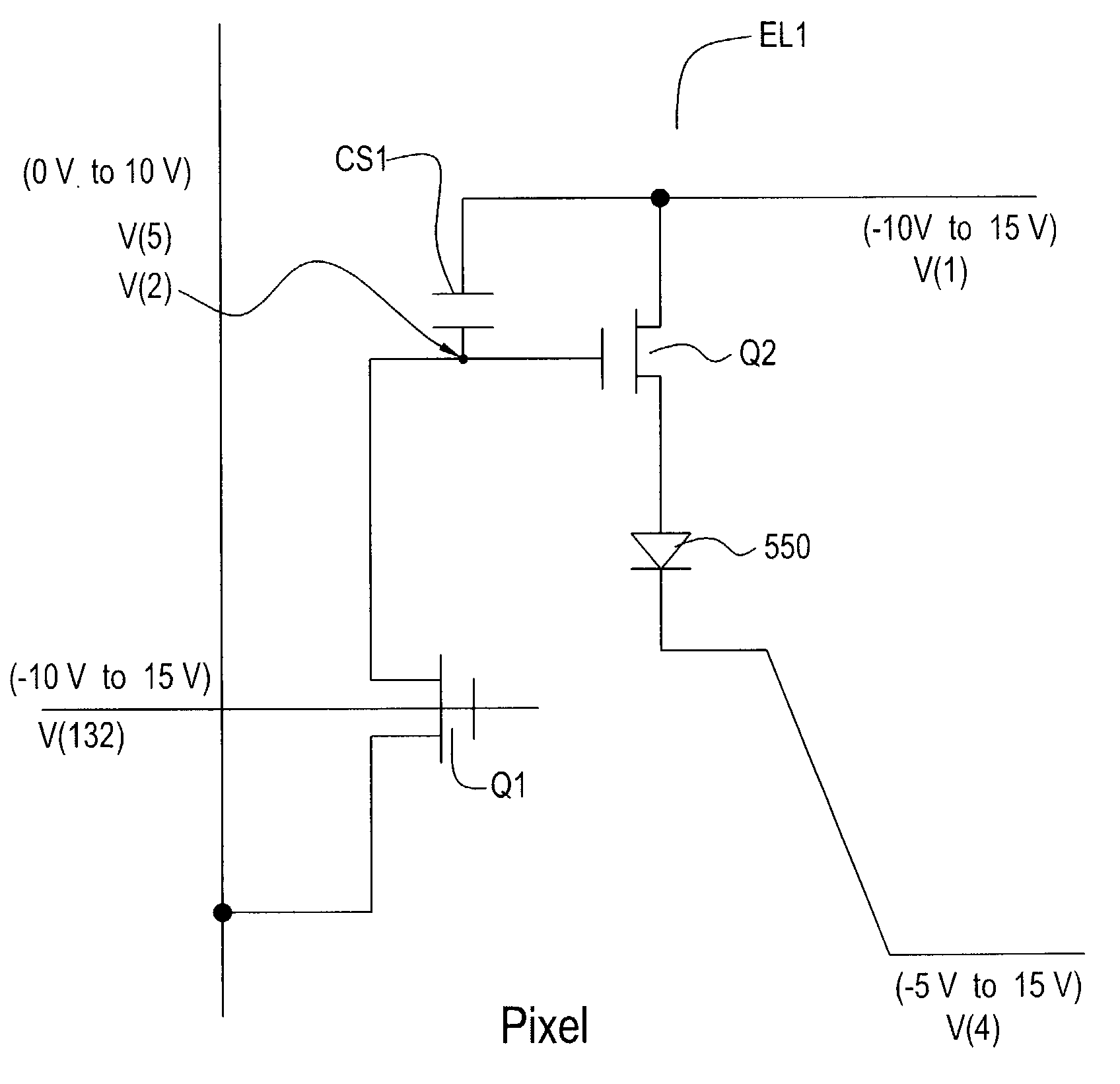
[0034]The present invention relates to an AMOLED pixel circuit having four modes of operation, namely (1) fast data sample and hold mode, (2) sufficient drive (illumination) current mode, (3) TFT threshold voltage compensation mode, and (4) OLED compensation mode. The circuit is configured with a minimal number of components thus allowing for a favorable aperture ratio.

[0035]The pixel circuit uses a-Si technology and incorporates several features: (1) the drains of driver transistor Q2 in a row, or group of rows, are tied together; (2) the power lines are brought out of the active matrix as a row line versus the Vsupply lines that are brought out as column lines, and (3) Vdata is a pulsed signal. The present invention offers a simple implementation of a pixel circuit with only a few TFTs, and may provide a defacto pixel adaptation by a-Si TFT-OLED display makers.

[0036]FIG. 3 is a schematic of a circuit 300 for an active matrix in accordance with the present invention. Circuit 300 in...


PUM


Abstract

There is provided a circuit for driving a current mode light modulating device. The circuit includes (a) a capacitor for storing a data voltage, (b) a field effect transistor (FET) controlled by a signal on a scan line, for coupling the data voltage from a signal line to the capacitor, and (c) a current source, controlled by the stored data voltage, for driving the device with current provided from a power line. The power line is in a plane that is geometrically parallel to a plane within which the scan line is located.

Description

CROSS REFERENCE TO RELATED APPLICATIONS[0001]The present application is claiming priority of U.S. Provisional Patent Application Ser. No. 60 / 332,389, filed on Nov. 20, 2001.BACKGROUND OF THE INVENTION[0002]1. Field of the Invention[0003]The present invention relates to a pixel circuit, and more particularly, to an active matrix organic light emitting diode (AMOLED) pixel circuit that can be implemented with amorphous silicon thin film transistors.[0004]2. Description of the Prior Art[0005]Several conventional active matrix drive schemes that have been used in liquid crystal display (LCDs) and are being investigated for use in AMOLEDs. These schemes include, for example, (1) an area ratio gray scale (ARG) method (M. Kimura, et al, Seiko Epson Corp., Japan, AMLDC2000), (2) a pulse width modulation method (S. Miyaguchi, et al, J. of SID, 7(3), 1999, p. 221–226), and (3) an amplitude modulation method, as used in direct view active matrix liquid crystal displays (AMLCDs).[0006]A display...

Claims


Application Information

Patent Timeline
Patent Type & Authority Patents(United States)
IPC IPC(8): G09G5/00G09G3/20G09G3/32
CPCG09G3/3233G09G3/2011G09G3/2014G09G2300/0426G09G2320/043G09G2310/0205G09G2310/0254G09G2310/0256G09G2300/0842
Inventor LIBSCH, FRANK RSANFORD, JAMES L
Owner INNOLUX CORP
Why Eureka
Try Eureka