Structure and method to minimize regrowth and work function shift in high-k gate stacks

a technology of high-k gate stack and work function, applied in the field of semiconductor devices, can solve the problems of reducing the work function prone to regrowth of the high-k gate material, and identifying materials for a dual work function metal gate electrode system, and achieve the effect of minimizing the threshold voltage shi

Inactive Publication Date: 2012-12-04
ALSEPHINA INNOVATIONS INC
View PDF2 Cites 1 Cited by
  • Summary
  • Abstract
  • Description
  • Claims
  • Application Information

AI Technical Summary

Benefits of technology

[0006]The present invention addresses the needs described above by providing a method of fabricating high-k material semiconductor structures in which regrowth of the high-k material is prevented and threshold voltage shifts are minimized. Further, the resulting semiconductor structures comprise high-k material regions that are self-aligned with respect to the active areas in the semiconductor substrate.

Problems solved by technology

In conventional high-k gate CMOS fabrication, the high-k material of the gate stack, specifically hafnium oxide dielectrics, are prone to re-growth.
Further, the workfunction of the high-k gate material may shift if the high-k material is exposed to oxygen during processing or comes into contact with oxygen-containing materials, such as silicon dioxide, SiO2.
So far, identification of materials for a dual work function metal gate electrode system has presented some challenges.
Moreover, finding high k gate stack materials suitable for gate first applications where the dielectric materials are subjected to high thermal budgets is a challenge.
However, this technique would suffer the overlay and critical dimension variations inherent in photolithographic techniques.

Method used


Image

  • Structure and method to minimize regrowth and work function shift in high-k gate stacks
  • Structure and method to minimize regrowth and work function shift in high-k gate stacks
  • Structure and method to minimize regrowth and work function shift in high-k gate stacks

Examples


Embodiment Construction

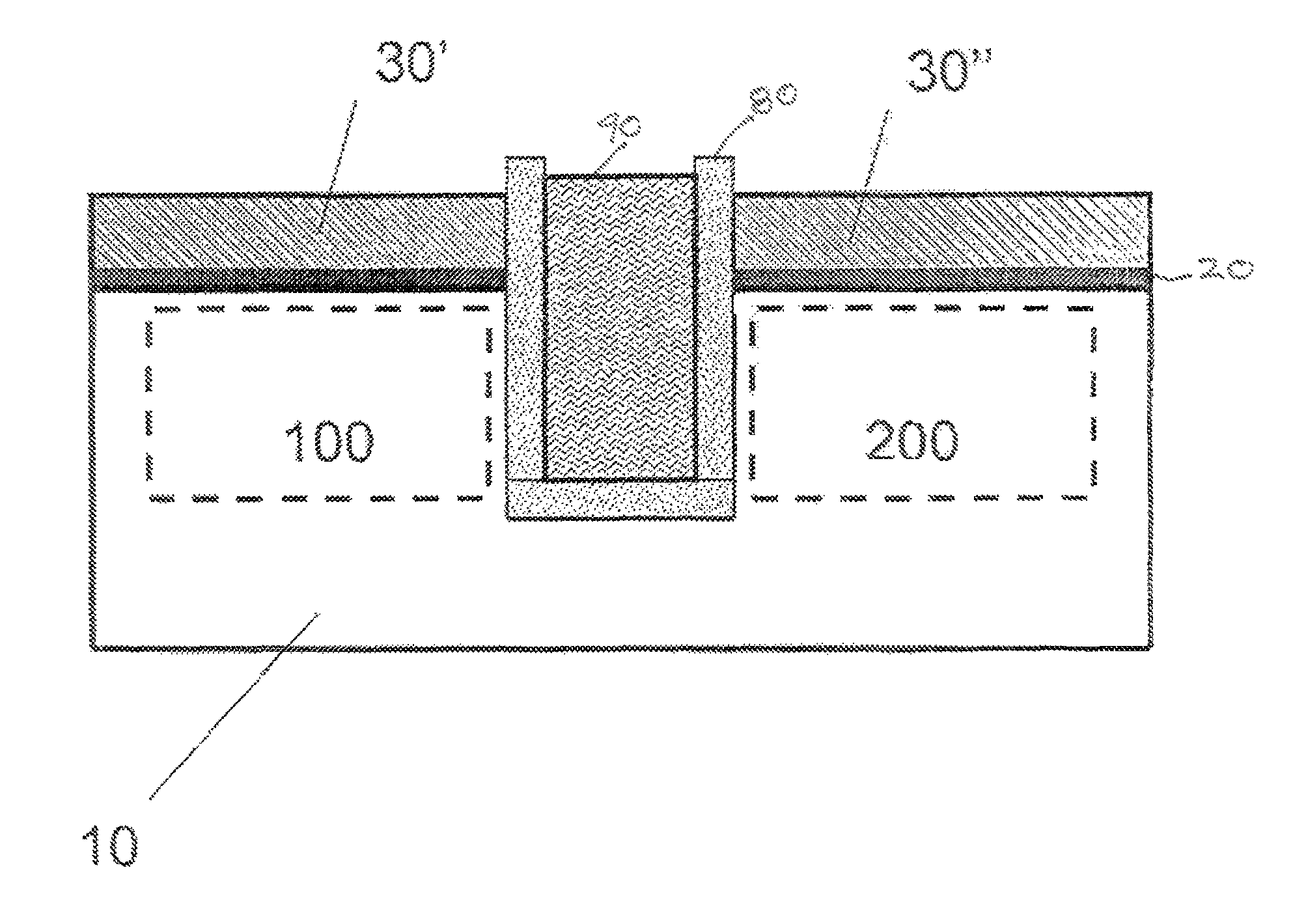
[0024]As stated above, the present invention relates to semiconductor structures having a high-k material portion. Such semiconductor structures are useful in the fabrication of semiconductor devices, for example, in the fabrication of complementary metal-oxide-semiconductor (CMOS). Semiconductor structures and methods of manufacturing the same are now described in detail with accompanying figures. The term “semiconductor structure” is used herein to refer to the semiconductor substrate and any subsequently formed structures on the semiconductor substrate. Thus, semiconductor structure may refer to, for example, to a semiconductor structure before and after a photoresist is applied onto the semiconductor structure.

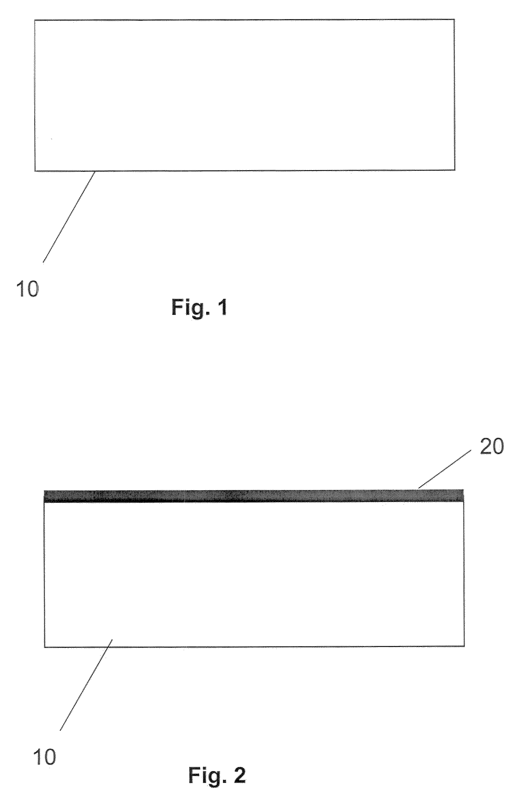
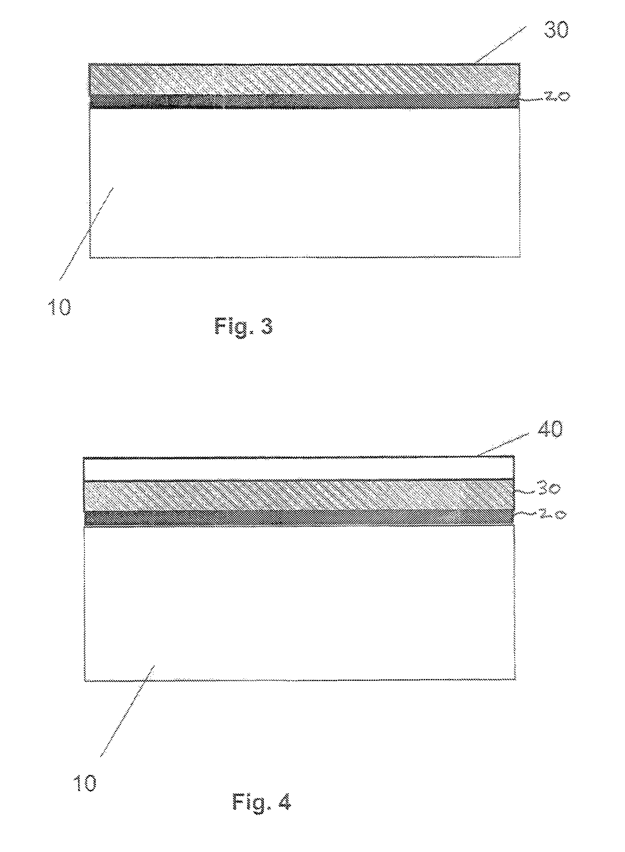
[0025]Referring to FIG. 1, a semiconductor substrate 10 is provided for fabricating a semiconductor structure. The semiconductor substrate 10 may be any semiconductor material and may be selected from, but is not limited to, silicon, germanium, silicon-germanium alloy, sil...


PUM


Abstract

The present invention provides a semiconductor structure comprising high-k material portions that are self-aligned with respect to the active areas in the semiconductor substrate and a method of fabricating the same. The high-k material is protected from oxidation during the fabrication of the semiconductor structure and regrowth of the high-k material and shifting of the high-k material work function is prevented.

Description

FIELD OF THE INVENTION[0001]The present invention generally relates to semiconductor devices, and particularly to semiconductor devices comprising high-k dielectric gate portions, and methods of manufacturing the same.BACKGROUND OF THE INVENTION[0002]Materials with a high dielectric constant, referred to herein as high-k materials or as high-k gate materials, are utilized in high-k gate complementary metal oxide semiconductor (CMOS) technology. In CMOS devices having a silicon channel, a conductive material having a work function of about 4.0 eV is necessary for n-type metal oxide semiconductor field effect transistors (NMOSFETs) and another conductive material having a work function of about 5.0 eV is necessary for p-type metal oxide semiconductor field effect transistors (PMOSFETs). In conventional high-k gate CMOS fabrication, the high-k material of the gate stack, specifically hafnium oxide dielectrics, are prone to re-growth. Further, the workfunction of the high-k gate materia...

Claims


Application Information

Patent Timeline
Patent Type & Authority Patents(United States)
IPC IPC(8): H01L21/76H01L29/06H01L21/762
CPCH01L21/76224H01L29/0649
Inventor CHENG, KANGGUODORIS, BRUCEKULKARNI, PRANITA
Owner ALSEPHINA INNOVATIONS INC
Why Eureka
Try Eureka