Method of modifying epitaxial growth shape on source drain area of transistor

a technology of source drain area and transistor, which is applied in the direction of semiconductor devices, basic electric elements, electrical equipment, etc., can solve the problems of merged adjacent epitaxial films and defect formation at the junction of the merged area,

Active Publication Date: 2016-02-11
APPLIED MATERIALS INC
View PDF4 Cites 31 Cited by
  • Summary
  • Abstract
  • Description
  • Claims
  • Application Information

AI Technical Summary

Benefits of technology

[0009]Methods for forming semiconductor devices, such as FinFETs, are provided. An epitaxial film is formed over a semiconductor fin, and the epitaxial film includes a top surface having two facets. A cap layer is deposited on the top surface, and portions of the epitaxial film in a lateral direction are removed. Having a smaller lateral dimension prevents the epitaxial film from merging with an adjacent epitaxial film and creates a gap between the epitaxial film and the adjacent epitaxial film.

Problems solved by technology

This may cause the reduction in the distance between an epitaxial film grown on a fin and an epitaxial film grown on an adjacent fin, which may cause adjacent epitaxial films to merge.
The merged epitaxial films decreases the effect of epitaxial films on the strain in the transistor channel, and defects may form easily at the junction of the merged area.

Method used


Image

  • Method of modifying epitaxial growth shape on source drain area of transistor
  • Method of modifying epitaxial growth shape on source drain area of transistor
  • Method of modifying epitaxial growth shape on source drain area of transistor

Examples


Embodiment Construction

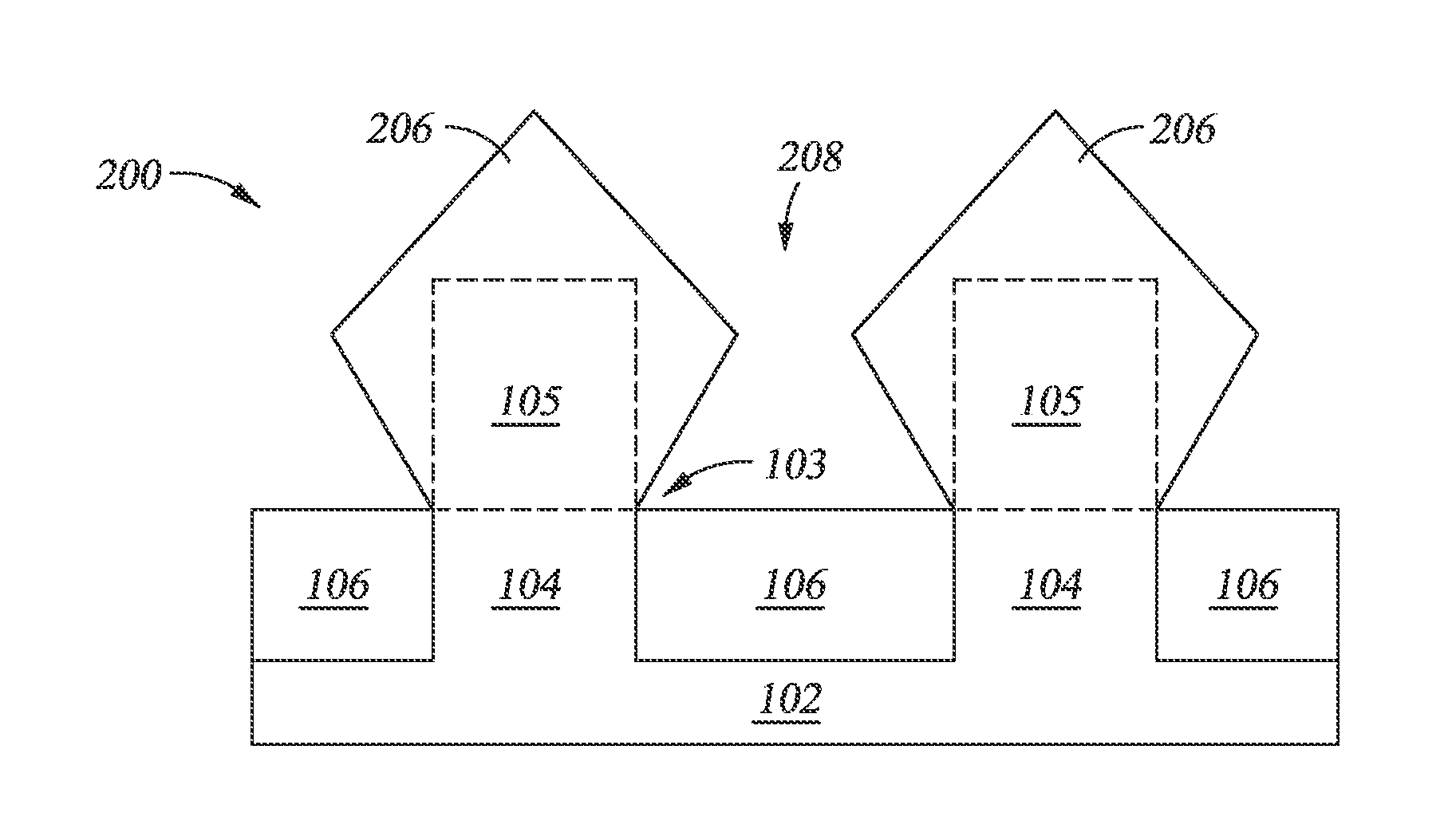
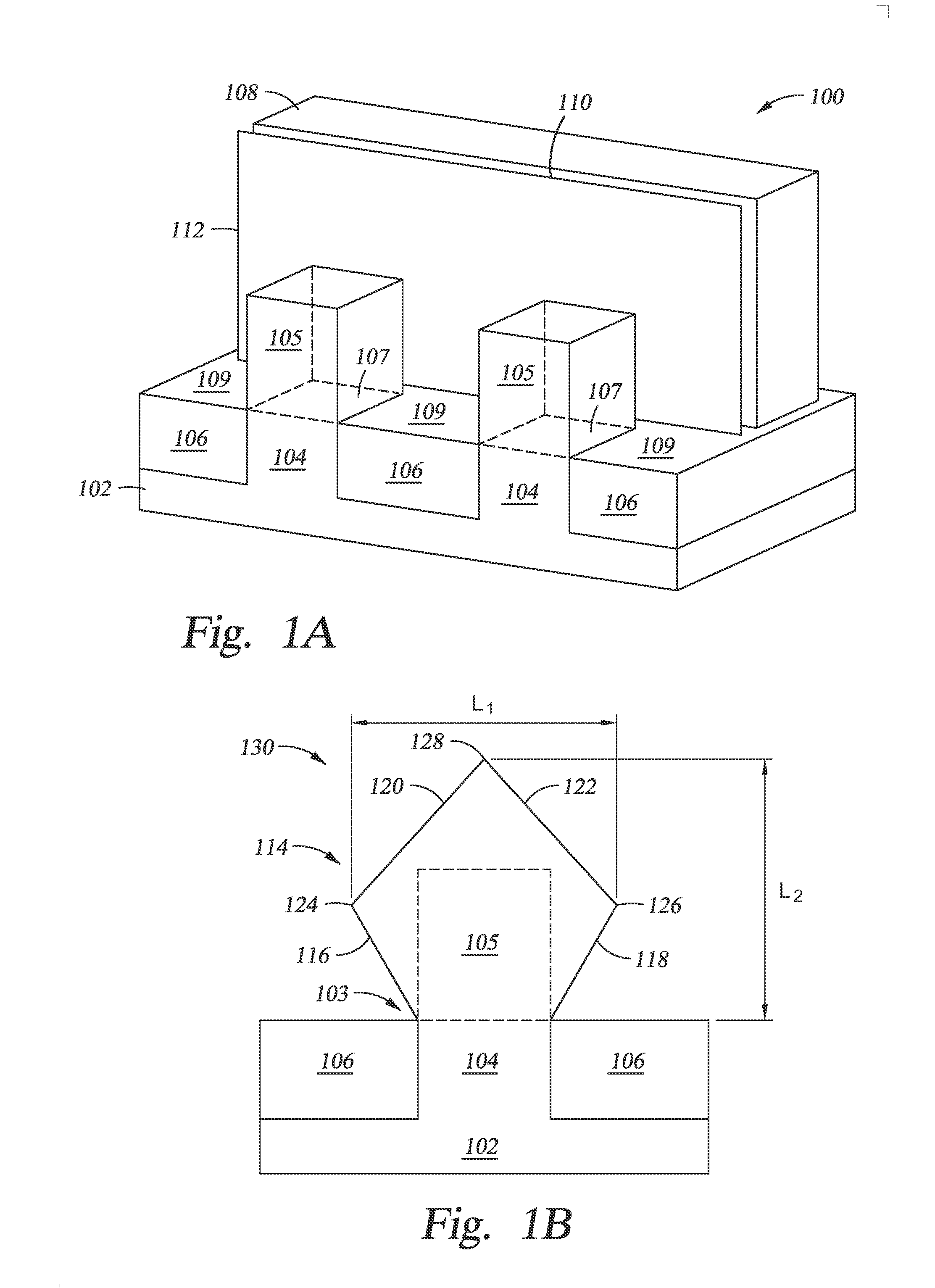
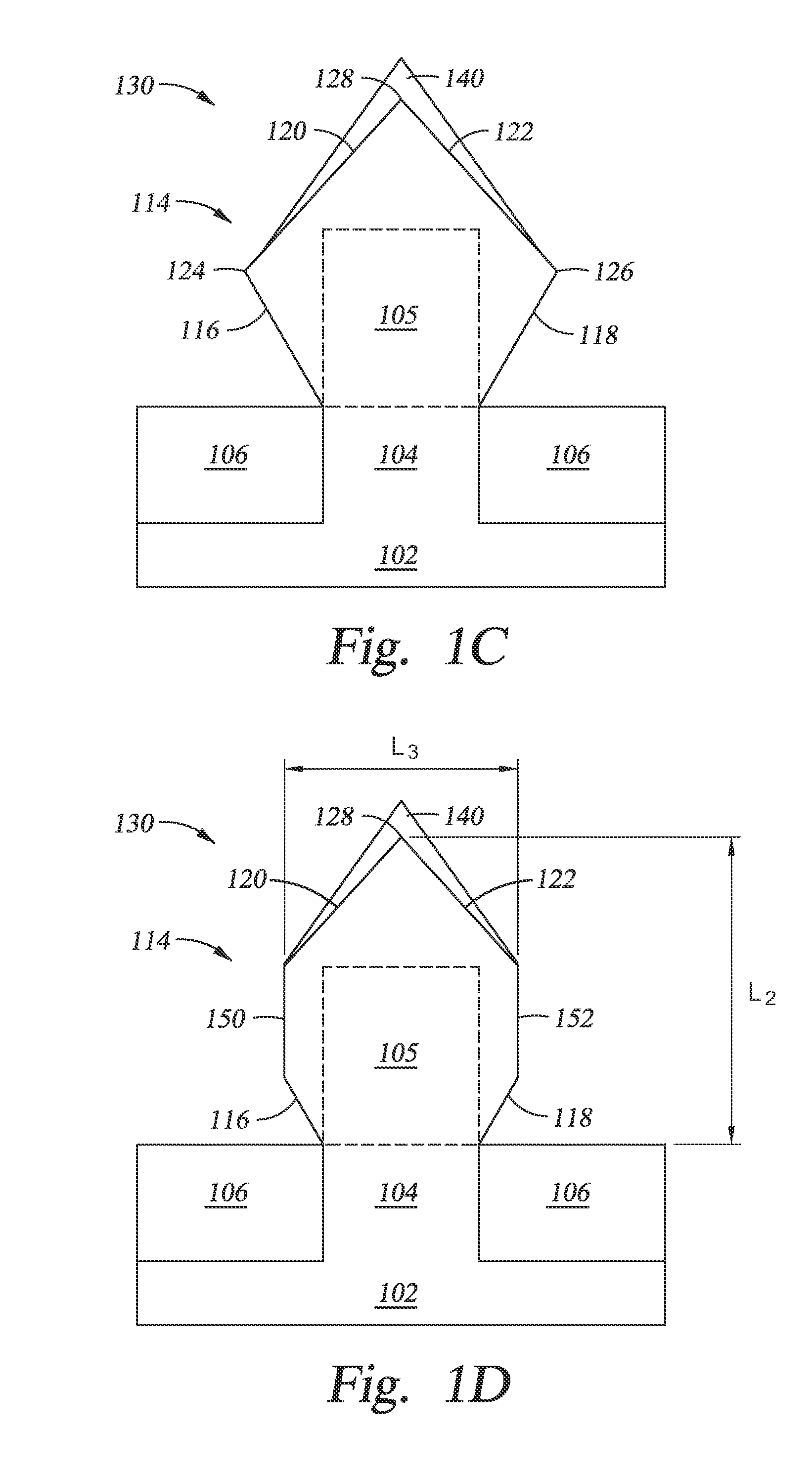
[0017]Methods for forming semiconductor devices, such as FinFETs, are provided. An epitaxial film is formed over a semiconductor fin, and the epitaxial film includes a top surface having two facets. A cap layer is deposited on the top surface, and portions of the epitaxial film in a lateral direction are removed. Having a smaller lateral dimension prevents the epitaxial film from merging with an adjacent epitaxial film and creates a gap between the epitaxial film and the adjacent epitaxial film.

[0018]FIGS. 1A-1D illustrate a process for forming a semiconductor device according to one embodiment described herein. FIG. 1A is a perspective view of a semiconductor structure 100. The semiconductor structure 100 may include a substrate 102, a plurality of semiconductor fins 103 (only two are shown), a dielectric material 106 disposed between the semiconductor fins 103 on the substrate 102, and a gate electrode 108 disposed on the dielectric material 106 and over a portion of each semicond...


PUM


Abstract

Methods for forming semiconductor devices, such as FinFETs, are provided. An epitaxial film is formed over a semiconductor fin, and the epitaxial film includes a top surface having two facets. A cap layer is deposited on the top surface, and portions of the epitaxial film in a lateral direction are removed. Having a smaller lateral dimension prevents the epitaxial film from merging with an adjacent epitaxial film and creates a gap between the epitaxial film and the adjacent epitaxial film.

Description

CROSS-REFERENCE TO RELATED APPLICATIONS[0001]This application claims priority to U.S. Provisional Patent Application Ser. No. 62 / 033,700, filed on Aug. 6, 2014, which herein is incorporated by reference.BACKGROUND[0002]1. Field[0003]Embodiments described herein generally relate to methods for forming semiconductor devices, and more particularly to methods for forming fin field effector transistors (FinFETs).[0004]2. Description of the Related Art[0005]As circuit densities increase for next generation devices, the widths of interconnects, such as vias, trenches, contacts, gate structures and other features, as well as the dielectric materials therebetween, decrease to 22 nm or smaller dimensions, whereas the thickness of the dielectric layers remain substantially constant, with the result of increasing the aspect ratios of the features. Recently, complementary metal oxide semiconductor (CMOS) FinFET devices have been widely used in many logic and other applications and are integrated...

Claims


Application Information

Patent Timeline
Patent Type & Authority Applications(United States)
IPC IPC(8): H01L21/308H01L21/02H01L29/08H01L29/66
CPCH01L21/3083H01L29/66795H01L29/0847H01L21/0262H01L21/02576H01L21/02579H01L21/02639H01L21/02598H01L21/02634H01L21/823431H01L21/02532
Inventor KIM, YIHWANLI, XUEBINDUBE, ABHISHEK
Owner APPLIED MATERIALS INC
Why Eureka
Try Eureka