Method of fabricating bottle trench capacitors using an electrochemical etch with electrochemical etch stop

a technology of trench capacitors and electrochemical etching, which is applied in the direction of semiconductor devices, basic electric elements, electrical apparatus, etc., can solve the problems of reducing the ability of gaseous etching species impinging from outside the trench to strike the outer portions of the trench bottom, reducing the effective time that the trench is exposed to liquid etching, and reducing the risk of merging adjacent trenches during processing. , the effect of minimizing the capacitance variation between th

Inactive Publication Date: 2005-11-03
KUDELKA STEPHAN P
View PDF18 Cites 5 Cited by
  • Summary
  • Abstract
  • Description
  • Claims
  • Application Information

AI Technical Summary

Benefits of technology

[0014] The present invention relates to structures and processes that improve storage capacitors. In particular, a process is disclosed that overcomes present limitations on production of trench capacitors. An exemplary embodiment of the current invention comprises a bottle trench capacitor structure formed by selective removal of a uniform sacrificial silicon layer of pre-determined thickness from the lower part of the trench. An object of the present invention is to produce bottle trench capacitors in a manner such that the risk of merging adjacent trenches during processing is minimized. This is accomplished in an exemplary embodiment of the current invention by use of a selective chemical etch with a built-in electrochemical etch stop. A bilayer region of silicon in the trench structure is formed such that the surface layer is removed under electrochemical etch without removal of the bottom layer. In this manner the amount of silicon removed from the trenches can be limited, and the problem of merging of adjacent trenches is avoided.
[0015] A further aspect of the present invention relates to the production of trenches of uniform size, such that the capacitance variation between trench devices is minimized. It is well known to those skilled in the art that, in addition to variation in dielectric layer thickness, the primary influence on trench capacitance is the internal trench surface area, which is, in turn, directly proportional to the trench size. In exemplary embodiments of the current invention, the final trench size is in large part determined by removal of a sacrificial silicon layer of well-controlled thickness as detailed below. This results in capacitors of more uniform dimension compared to those produced by conventional processes. An additional object of the current invention is the fabrication of trenches with maximum capacitance attainable for a given DRAM cell size and trench separation. It will be appreciated by those skilled in the art that the more uniform process contained in embodiments of the present invention makes it possible to increase the average trench width without increased risk of failure due to merging of trenches.

Problems solved by technology

However, as the total cell size is reduced, the amount of charge retained in a horizontal planar capacitor may not be sufficient to ensure proper device operation, since the capacitance is directly proportional to the planar area of the device.
The tapering is due in part to the increased ratio of depth to width in the trenches as they are etched deeper, which reduces the ability of the gaseous etching species impinging from outside the trench to strike the outer portions of the trench bottom.
Additionally, control of the effective time that the trench is exposed to liquid etchant may be difficult.
However, the extremely small size and bottle shape of the trenches can act to retard liquid etchant removal, resulting in an effective etch time greater than desired.
In addition, the etch profile within a trench may not be uniform, due to incomplete or tardy removal of liquid etchant in certain regions such as comers in the trench.
For the above reasons, among others, the uniformity of trench size may be difficult to control, and can lead to failures where adjacent bottle trenches merge, as depicted in FIG. 4. FIG. 4 illustrates an array of equally-spaced bottle trenches 31, 32, 33, and 34 after bottle etch and rinse.
A further problem with the bottle etch process described in related art is that the nonunifomity can lead to significantly lower than ideal trench capacitance.

Method used


Image

  • Method of fabricating bottle trench capacitors using an electrochemical etch with electrochemical etch stop
  • Method of fabricating bottle trench capacitors using an electrochemical etch with electrochemical etch stop
  • Method of fabricating bottle trench capacitors using an electrochemical etch with electrochemical etch stop

Examples


Embodiment Construction

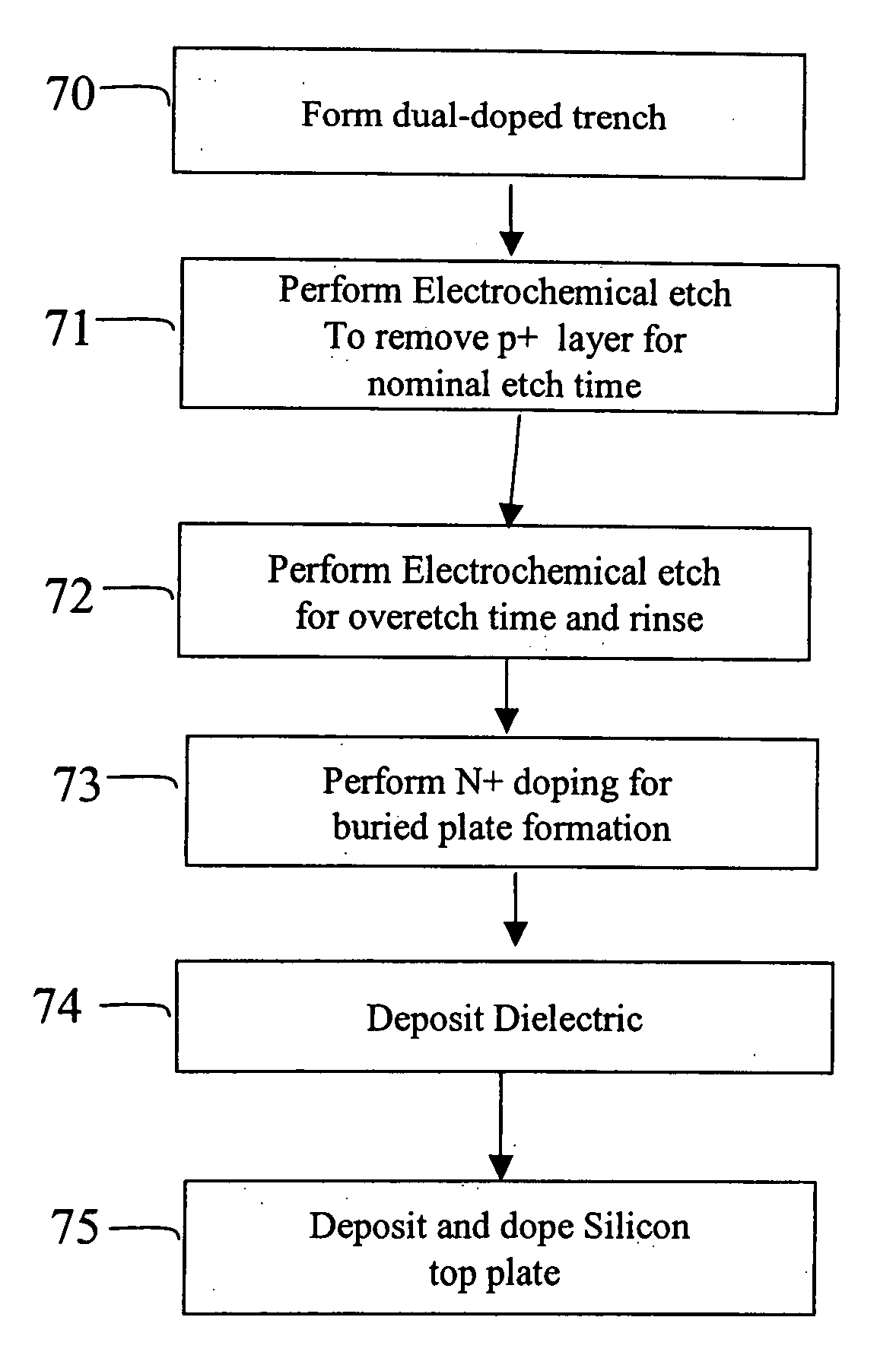
[0025] Preferred embodiments of the present invention are described below, with reference made to the enclosed drawings. Before one or more embodiments of the invention are described in detail, one skilled in the art will appreciate that the invention is not limited in its application to the details of trench structure and the arrangement of steps set forth in the following detailed description or illustrated in the drawings. The invention is capable of other embodiments and of being practiced or being carried out in various ways. Also, it is to be understood that the phraseology and terminology used herein is for the purpose of description and should not be regarded as limiting.

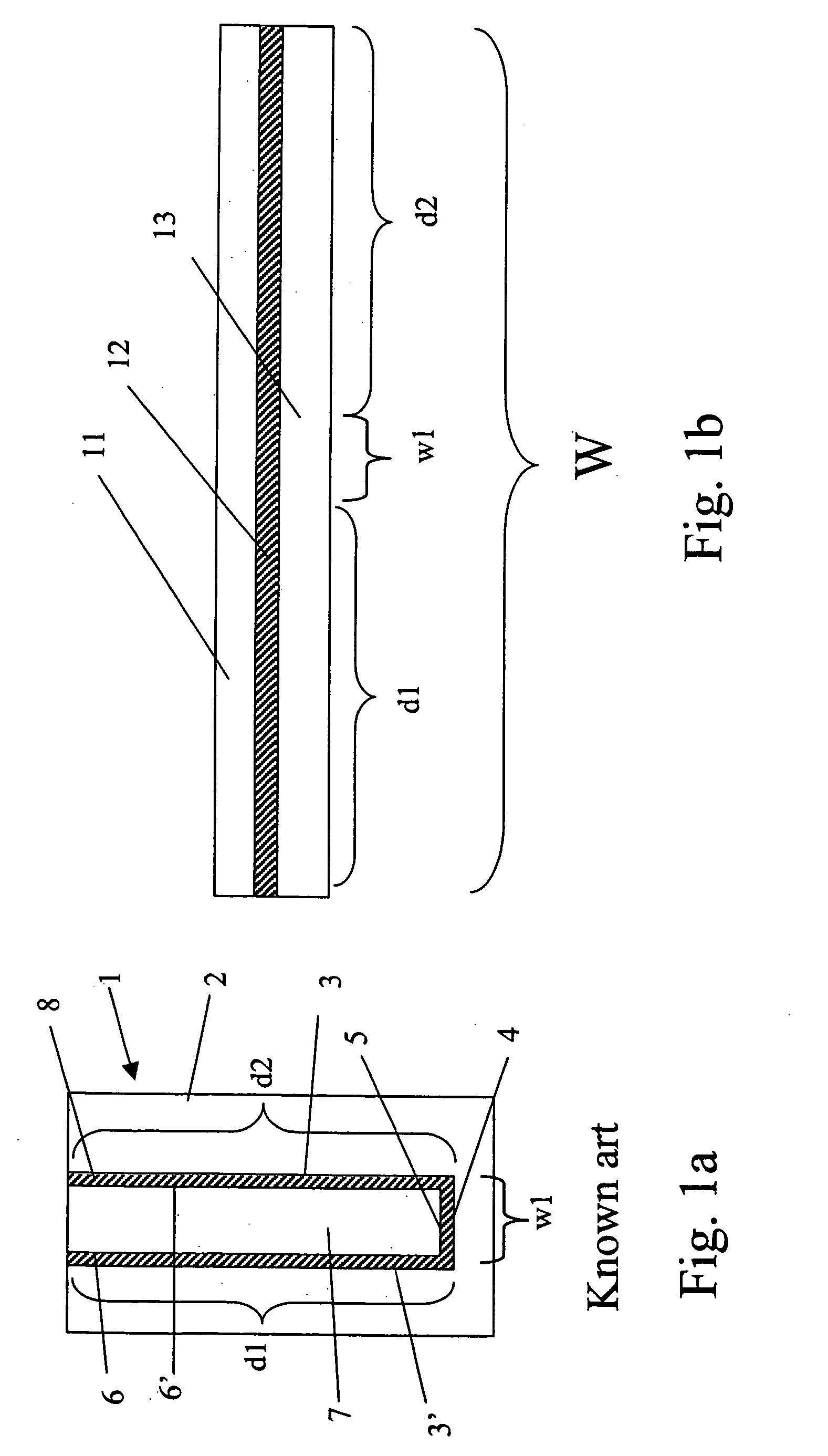
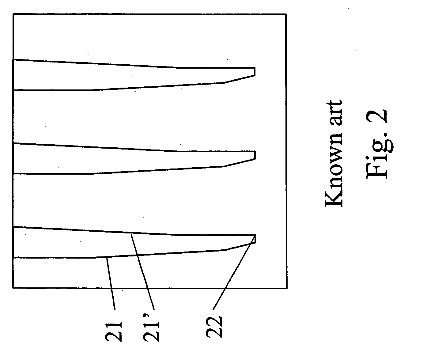
[0026] The present invention is related to methods and structures for providing large and uniform DRAM trench capacitors. Current methods of bottle trench capacitor fabrication employ non-selective wet etching of silicon to enlarge the trench below a collar region. This process entails the risk of complete ...


PUM

PropertyMeasurementUnit
depthaaaaaaaaaa
depthaaaaaaaaaa
widthaaaaaaaaaa

Abstract

A method of forming trench capacitors in, e. g., a DRAM device, using an electrochemical etch with built-in etch stop to fabricate well-defined bottle-shaped capacitors is described. The process includes formation of a sacrificial silicon layer after initial deep trench formation, wherein the sacrificial layer is formed by doping, and upon its removal, a bottle trench is formed. A second region of doped silicon located below the sacrificial layer is resistant to the chemical etch performed to remove the sacrificial layer, and thereby renders the bottle trench formation process self-limiting.

Description

BACKGROUND OF THE INVENTION [0001] 1. Field of the Invention [0002] The present invention relates generally to semiconductor devices. More particularly, the present invention relates to methods of making and the structure of trench capacitors in memory devices. [0003] 2. Background Information [0004] The semiconductor industry requires miniaturization of individual devices such as transistors and capacitors to accommodate the increasing density of circuits necessary for semiconductor products. One common semiconductor product is a dynamic random access memory (“DRAM”), which may incorporate billions of individual DRAM memory units (cells), each capable of storing one data bit. A DRAM cell includes a planar access transistor and a storage capacitor. The access transistor transfers charge to and from the storage capacitor to read or write data. The total amount of charge stored in the capacitor must exceed a threshold value, which is based on the minimum amount of charge required to r...

Claims


Application Information

Patent Timeline
Patent Type & Authority Applications(United States)
IPC IPC(8): C25F3/12H01L21/20H01L21/3063H01L21/82H01L21/8242
CPCC25F3/12H01L27/1087H01L21/3063H10B12/0387
Inventor KUDELKA, STEPHAN P.
Owner KUDELKA STEPHAN P
Why Eureka
Try Eureka