Supercharge Your Innovation With Domain-Expert AI Agents!

MEMS devices and method of manufacturing

a technology of mems and manufacturing method, applied in the direction of fluid speed measurement, instruments, coatings, etc., can solve the problems of limiting the cost of production, the wafer cannot be processed using standard wafer handling tooling, and the cost of production increases

Inactive Publication Date: 2016-02-25
ROSEMOUNT AEROSPACE
View PDF3 Cites 3 Cited by
  • Summary
  • Abstract
  • Description
  • Claims
  • Application Information

AI Technical Summary

Benefits of technology

This patent describes a MEMS sensor that includes a sensor die and a pedestal layer. The pedestal layer has a channel that is around a pedestal and can define the shape of the sensor. The size of the channel can be either cylindrical or rectangular, and the depth of the channel can be half the thickness of the layer. The remainder of the layer is outside the channel and can have the same material as the sensor die. The method for manufacturing the sensor involves disposing the pedestal layer on a sensor layer and then creating a channel for each sensor die using chemical etching or machining. The sensor can also have a fluid port and a remainder portion outside the channel. The technical effects of this design include improved signal quality and reduced noise, as well as improved manufacturing precision and reliability.

Problems solved by technology

Presently, each pedestal is manually placed on each die defined on the wafer which adds cost and processing time.
Also, once each pedestal is attached, the wafer can no longer be processed using standard wafer handling tooling.
The die spacing is a limiting factor on cost of production.

Method used


Image

  • MEMS devices and method of manufacturing
  • MEMS devices and method of manufacturing

Examples


Embodiment Construction

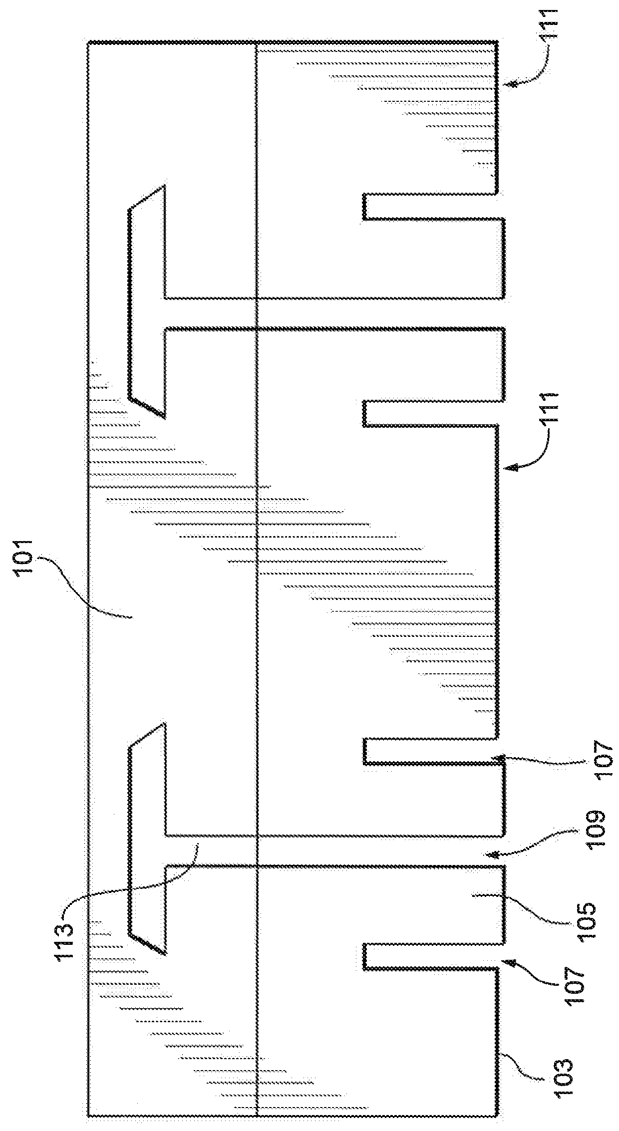
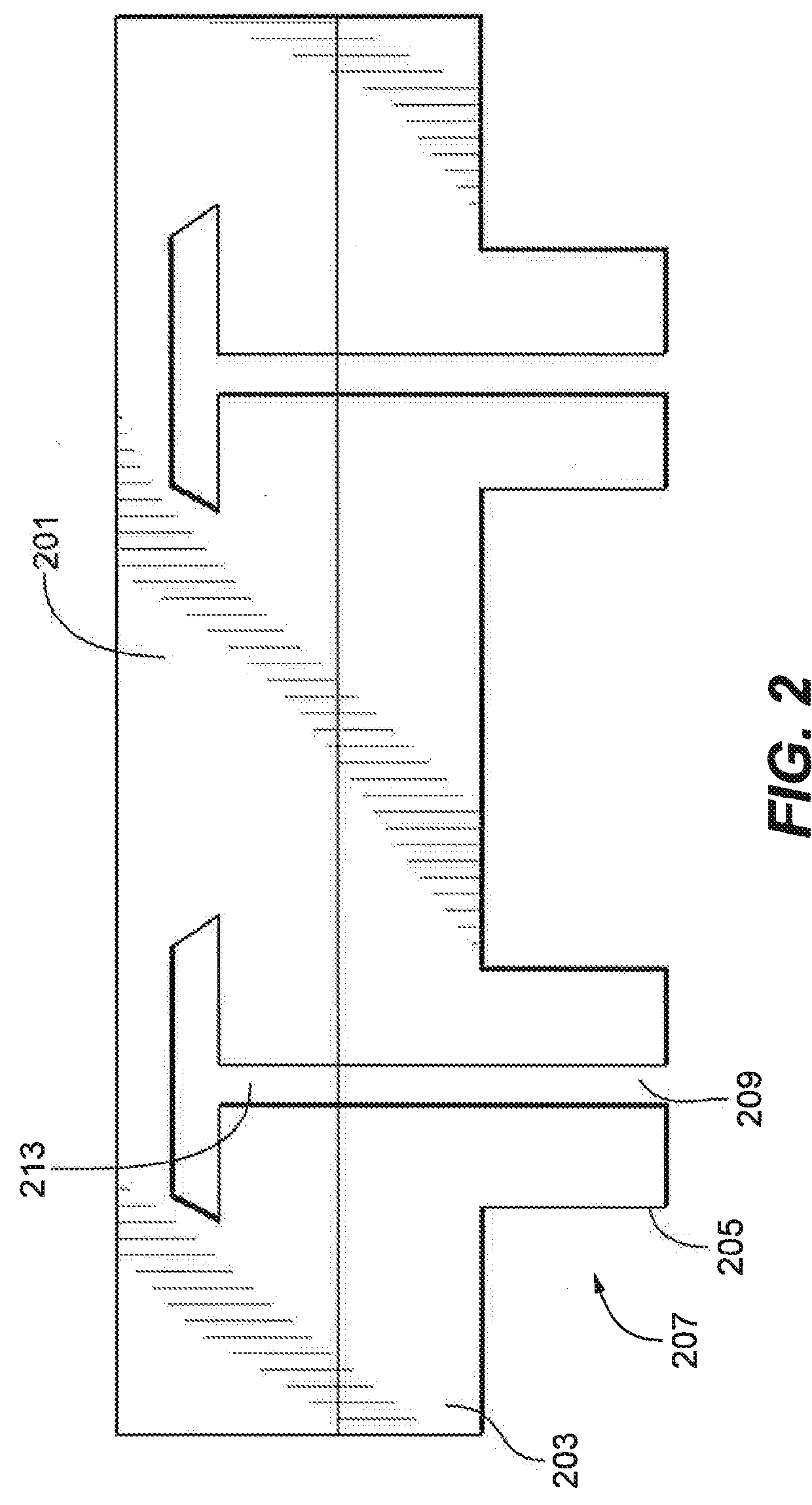
[0018]Reference will now be made to the drawings wherein like reference numerals identify similar structural features or aspects of the subject disclosure. For purposes of explanation and illustration, and not limitation, an illustrative view of an embodiment of a MEMS sensor wafer in accordance with the disclosure is shown in FIG. 1 and is designated generally by reference character 100. Another embodiment of a MEMS sensor wafer is shown in FIG. 2. The systems and methods described herein can allow bulk manufacture of MEMS sensors more efficiently.

[0019]In at least one aspect of this disclosure, a MEMS sensor (e.g., half of MEMS sensor wafer 100 as shown) includes a sensor die 101 (shown in a layer during manufacture) configured to generate a sensor signal and a pedestal layer 103 disposed on the sensor die 101. The pedestal layer 103 includes a channel 107 defined therein about a pedestal 105 of the pedestal layer 103. The pedestal 105 is configured to be mounted to a housing (not...


PUM

PropertyMeasurementUnit
aspect ratioaaaaaaaaaa
cylindrical shapeaaaaaaaaaa
rectangular shapeaaaaaaaaaa

Abstract

A MEMS sensor includes a sensor die configured to generate a sensor signal and a pedestal layer disposed on the sensor die. The pedestal layer includes a channel defined therein about a pedestal of the pedestal layer. The pedestal is configured to be mounted to a housing. A method for manufacturing MEMS sensors can include disposing a pedestal layer on a sensor layer, wherein the sensor layer defines a plurality of sensor dies to be cut therefrom. The method further includes defining a respective channel in the pedestal layer for each sensor die, thereby creating a pedestal for each sensor die.

Description

BACKGROUND[0001]1. Field[0002]The present disclosure relates to micro electromechanical systems (MEMS), more particularly to MEMS devices used as sensors.[0003]2. Description of Related Art[0004]MEMS sensors can be bulk manufactured as wafers which are divided through cutting the wafer. Stress isolation in MEMS sensors can be achieved by attaching one or more pedestals to each sensor die to mount the sensor die to the housing of the MEMS device. Physical stresses acting upon the MEMS sensors are translated to the pedestal without transferring the stresses to the sensor die. Presently, each pedestal is manually placed on each die defined on the wafer which adds cost and processing time. Also, once each pedestal is attached, the wafer can no longer be processed using standard wafer handling tooling. Instead, custom fixtures with recesses for the pedestals are needed for further processing. Additionally, die spacing is increased to accommodate the specialized tooling, thereby reducing ...

Claims


Application Information

Patent Timeline
Patent Type & Authority Applications(United States)
IPC IPC(8): B81C1/00B81B7/00
CPCB81C1/00873B81C1/00492B81B7/0061B81B7/0048
Inventor POTASEK, DAVID, P.
Owner ROSEMOUNT AEROSPACE
Features
  • R&D
  • Intellectual Property
  • Life Sciences
  • Materials
  • Tech Scout
  • Unparalleled Data Quality
  • Higher Quality Content
  • 60% Fewer Hallucinations
Learn More