

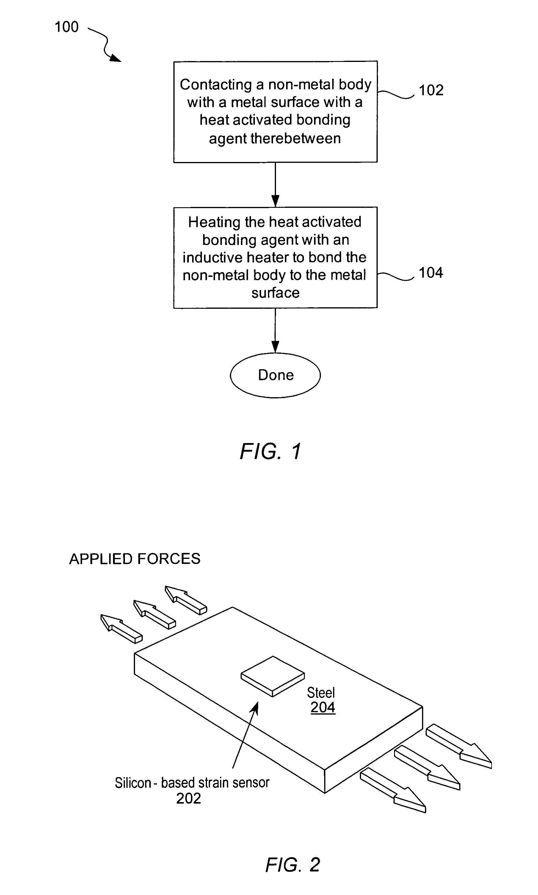
Bonding a non-metal body to a metal surface using inductive heating
a non-metal body and metal surface technology, applied in the direction of microstructural technology, solid-state devices, microstructure devices, etc., can solve the problems of long-term creep of bonds, many intrinsic limitations of these techniques, and the use of silicon sensors in bonding steel, etc., to avoid any detrimental change in material properties of metal surfaces, fast and effective bonding
- Summary
- Abstract
- Description
- Claims
- Application Information
AI Technical Summary
Benefits of technology
Problems solved by technology
Method used
Image

Examples
example 1
Silicon to Steel Bonding and Testing
[0048]The process overview for the tests performed is shown in FIG. 4, described more generally above to address more general features of the invention. Two different basic processes were tested, each with a different solder. The first approach (Method 1) utilized lead-free solder paste and various adhesion layer systems. Silicon wafers with thicknesses of 550 μm, 300 μm, and 100 μm were cleaned in a Piranha bath (100:1, Sulfuric Acid:Hydrogen Peroxide at 120° C.) for 10 minutes, and a seed layer of chromium and copper was evaporated to the polished surfaces of the wafers. Nickel was then electroplated to the wafers, along with a very thin layer of Pb / Sn solder to prevent the nickel from oxidizing. Although a leaded solder was used in these experiments to serve as an oxidation barrier, a comparable, electroplatable solder may also be used.
[0049]The two solders used for this work were 96.5Sn / 3Ag / 0.5Cu lead-free solder paste (Hi-Performance Lead-Fre...
example 2
Further Details of an Inductively Heated Silicon-to-Steel Bonding Protocol
The following protocol details for particular embodiments of the invention are applicable to the test processes described in Example 1:
[0057]1) Silicon Chip Preparation:[0058]a. Silicon wafers (10-50 Ω-cm resistivity, 100, p-type (B)1) are cleaned in Piranha bath (100:1, Sulfuric Acid:Hydrogen Peroxide at 120° C.) for 10 minutes[0059]b. An adhesion layer of one of the following sets is then deposited onto the wafer[0060]i. Evaporated 200 Å Chromium (or titanium) / Evaporated 1000 ÅGold—used with bonding method 1 (discussed below)[0061]ii. Evaporated 500 Å Chromium (or titanium) / Evaporated 7000 ÅSilver—used with bonding method 1 (discussed below)[0062]iii. Evaporated 200 Å Chromium (or titanium) / Evaporated 1000 ÅCopper / 2 μm Electroplated Nickel / 1 μm Electroplated Eutectic Pb / Sn Solder—used with bonding method 1 (discussed below)[0063]iv. Evaporated 200 Å Chromium (or titanium) / Evaporated 1000 ÅCopper / 2 μm Electro...
example 3
Hardness Testing
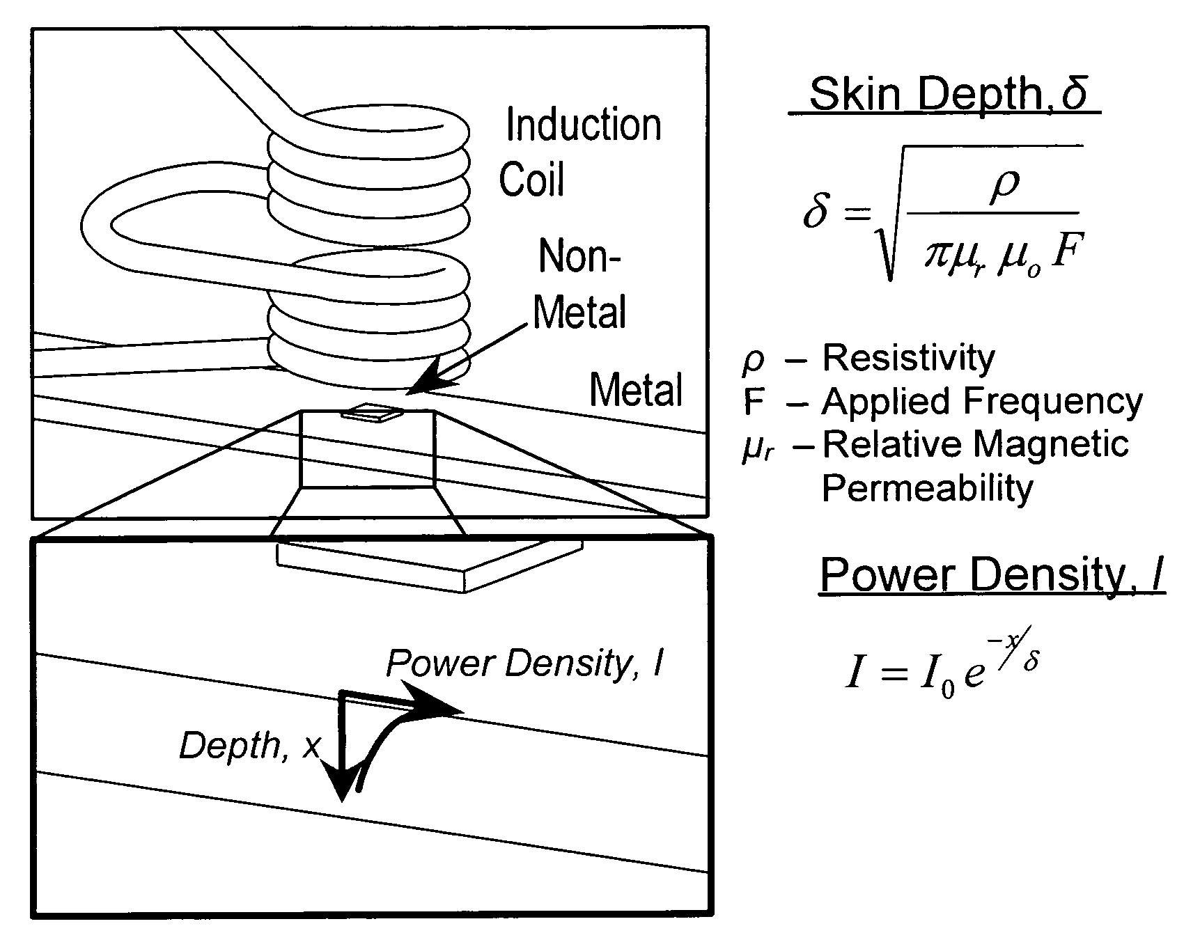
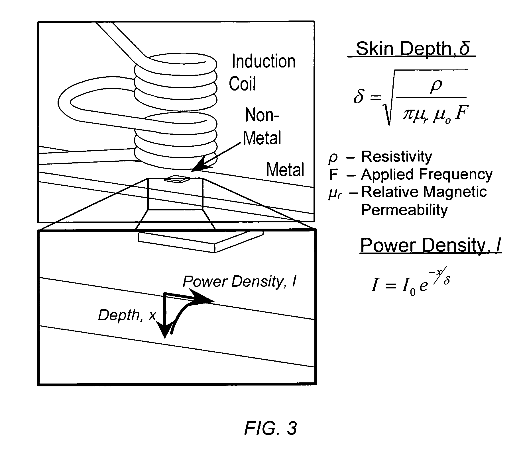
[0092]The bonding process has been demonstrated to do no damage to steel of a high hardness, for example as described below. Because of the nature of inductive heating, the alternating electromagnetic field penetrates the steel to a depth on the order of only a few microns. Therefore, the heat is essentially generated only at the steel surface from Joule heating, and the rest of the sample, although heated through conduction, can remain well below the temperatures at which heat treated steel begins to change. The damage to the steel was verified on a bearing steel race, whereby the hardness was measured before and after bonding the silicon chip to the race and the temperature at the steel surface was monitored with Tempilaq G Temperature Indicating Liquid paint. Preventing damage to the steel is important because the bonding of silicon chips to steel would generally be performed after the heat treatment to the steel in an industrial manufacturing process.
[0093]Hardne...
PUM
| Property | Measurement | Unit |
|---|---|---|
| pressure | aaaaa | aaaaa |
| pressure | aaaaa | aaaaa |
| surface roughness | aaaaa | aaaaa |
Abstract
Description
Claims
Application Information