Method to package multiple MEMS sensors and actuators at different gases and cavity pressures

a technology of microelectro mechanical systems and actuators, applied in the field of integrated electronic devices and systems, can solve the problems of unstable output signal of accelerometers, low operating pressure of conventional wafer-level packaging processes, and inability to provide single operating pressure across wafers, etc., to achieve the effect of reducing the number of overlapping processes

Active Publication Date: 2014-08-14
MOVELLA INC
View PDF3 Cites 57 Cited by
  • Summary
  • Abstract
  • Description
  • Claims
  • Application Information

AI Technical Summary

Benefits of technology

[0007]According to embodiments of the present invention, techniques generally related to integrated electronic devices and systems are provided. In particular, the present invention provides a method for packaging multiple MEMS sensors and actuators. Merely by way of example, the MEMS devices can include an accelerometer, a gyroscope, a magnetic sensor, a pressure sensor, a microphone, a humidity sensor, a temperature sensor, a chemical sensor, a biosensor, an inertial sensor, and others. But it will be recognized that the invention has a much broader range of applicability.
[0008]The performance of MEMS devices have been found to be highly dependent on their operation pressures. Different MEMS devices can have optimal operating pressures. For example, MEMS accelerometers may require a higher operating pressure to ensure their performance and reliability. At low pressures, a MEMS accelerometer could have non-ideal oscillations (“ringing”) under a sudden change of input acceleration, which makes the output signal of the accelerometer unstable. This non-ideal oscillation can be suppressed by increasing the air pressure of the environment around the accelerometer with a sealing gas, which can increase the damping of the accelerometer. High cavity pressure can also help to reduce the impact force due to the collision of the accelerometer's proof mass with the motion stoppers by acting as a damper and reducing the collision velocity.
[0009]On the other hand, resonance based sensors, such as gyroscopes and magnetometers, may require low operating pressures to minimize the damping during their operations. These sensors have larger sensitivities and lower power consumption at lower operation pressures. Similarly, MEMS resonators, which are used for oscillators and filters, may require low pressure to minimize damping as well or to maximize their quality factors. MEMS oscillators for timing reference applications need high quality factors to reduce the impact of close-to-carrier phase noise. MEMS filters may also require high quality factors for high frequency sensitivity. MEMS based infrared sensors, such as micro-bolometers may also require low operating pressures to minimize the thermal conduction through the surrounding gas and to maximize their sensitivity.
[0011]It is an object of the present invention to develop methods of fabricating integrated electronic devices that include different MEMS devices on one silicon chip or wafer. Integrating multiple MEMS devices on a single chip or wafer can reduce the die size and manufacturing costs. One of the difficulties of integrating different MEMS devices is the varying requirements of operational pressures, since conventional packaging methods cannot vary the sealing pressure from device to device. As seen from the above, it is an object of the present invention to develop a wafer-level packaging method that allows different devices, such as MEMS devices, to be sealed within different operation pressures on the same wafer or die.
[0016]Many benefits are achieved by way of embodiments the present invention over conventional techniques. For example, embodiments of the present technique provide an easy to use process to integrate a multiple different MEMS devices on a single die. In some embodiments, the method provides higher device yields in dies per wafer with the integrated approach. Additionally, the method provides a process and system that are compatible with conventional semiconductor and MEMS process technologies without substantial modifications to conventional equipment and processes. Preferably, the invention provides for an improved multi-MEMS systems and related applications for a variety of uses. Depending upon the embodiment, one or more of these benefits may be achieved. These and other benefits will be described in more throughout the present specification and more particularly below.

Problems solved by technology

At low pressures, a MEMS accelerometer could have non-ideal oscillations (“ringing”) under a sudden change of input acceleration, which makes the output signal of the accelerometer unstable.
However, conventional wafer-level packaging processes only provide a single operating pressure across a wafer.

Method used


Image

  • Method to package multiple MEMS sensors and actuators at different gases and cavity pressures
  • Method to package multiple MEMS sensors and actuators at different gases and cavity pressures
  • Method to package multiple MEMS sensors and actuators at different gases and cavity pressures

Examples


Embodiment Construction

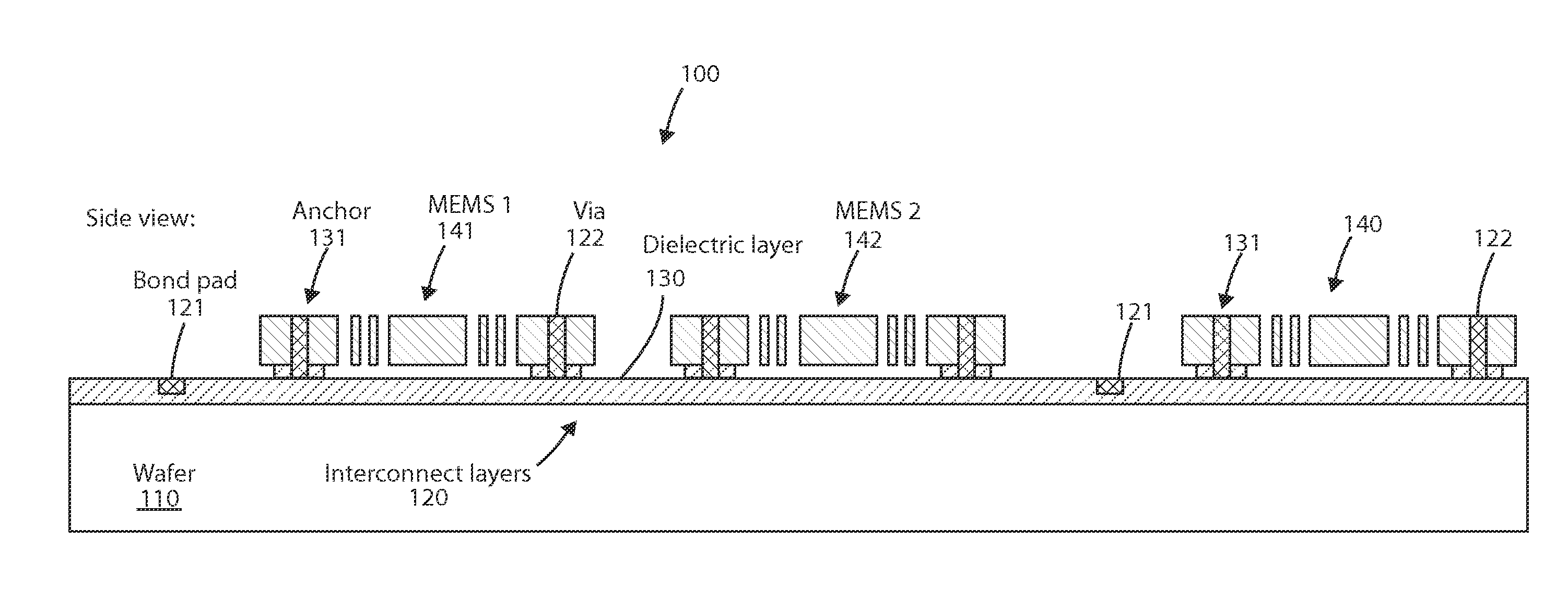
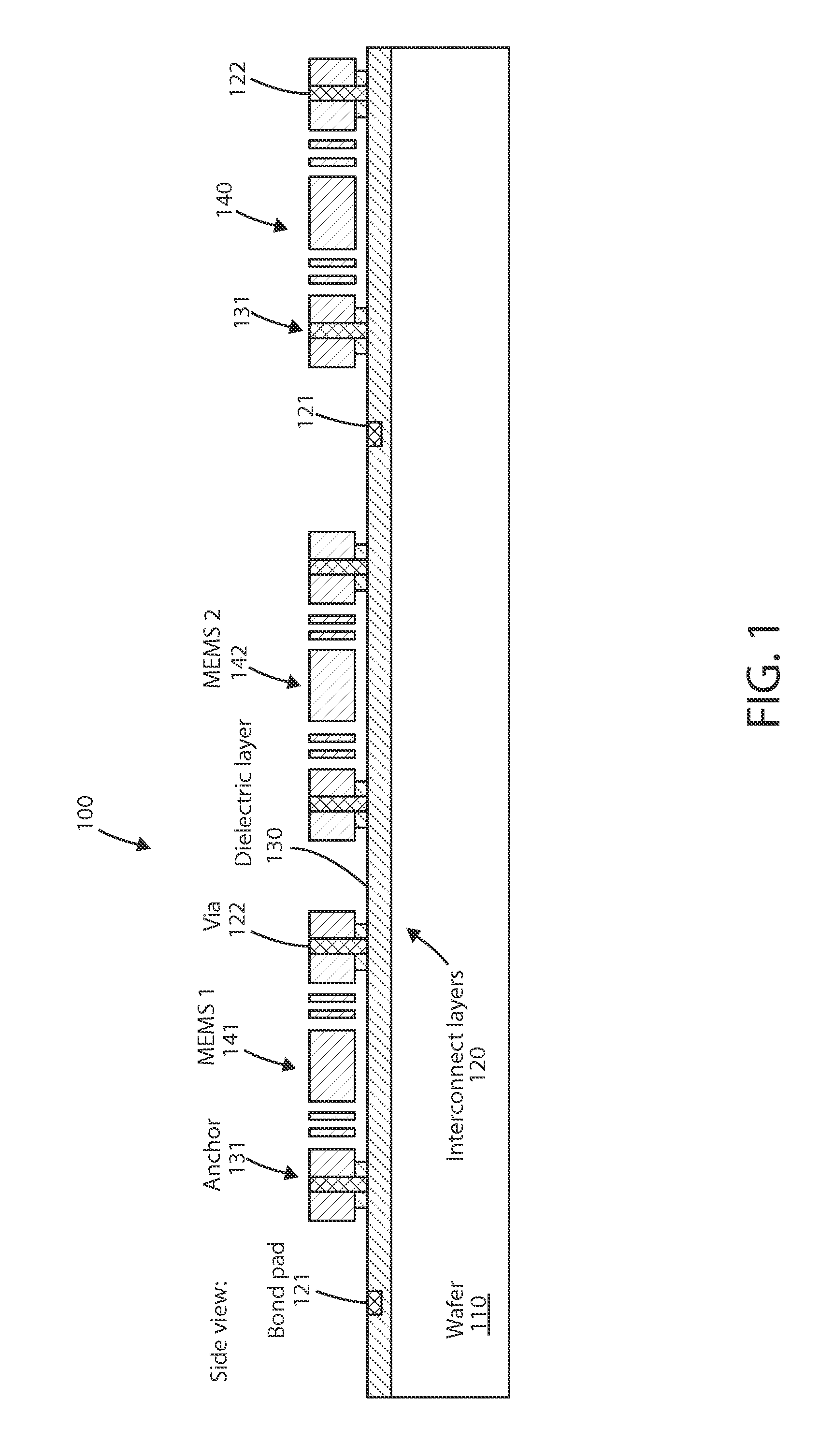
[0034]According to embodiments of the present invention, techniques generally related to integrated electronic devices and systems are provided. In particular, the present invention provides a method for packaging multiple MEMS sensors and actuators. Merely by way of example, the MEMS devices can include an accelerometer, a gyroscope, a magnetic sensor, a pressure sensor, a microphone, a humidity sensor, a temperature sensor, a chemical sensor, a biosensor, an inertial sensor, and others. But it will be recognized that the invention has a much broader range of applicability.

[0035]The performance of MEMS devices have been found to be highly dependent on their operation pressures. Different MEMS devices can have optimal operating pressures. For example, MEMS accelerometers may require a higher operating pressure to ensure their performance and reliability. At low pressures, a MEMS accelerometer could have non-ideal oscillations (“ringing”) under a sudden change of input acceleration, ...


PUM

PropertyMeasurementUnit
thickaaaaaaaaaa
air pressureaaaaaaaaaa
pressureaaaaaaaaaa

Abstract

A method for fabricating a multiple MEMS device. A semiconductor substrate having a first and second MEMS device, and an encapsulation wafer with a first cavity and a second cavity, which includes at least one channel, can be provided. The first MEMS can be encapsulated within the first cavity and the second MEMS device can be encapsulated within the second cavity. These devices can be encapsulated within a provided first encapsulation environment at a first air pressure, encapsulating the first MEMS device within the first cavity at the first air pressure. The second MEMS device within the second cavity can then be subjected to a provided second encapsulating environment at a second air pressure via the channel of the second cavity.

Description

CROSS-REFERENCES TO RELATED APPLICATIONS[0001]The present application claims priority to and incorporates by reference, for all purposes, the following pending patent application: U.S. Pat. App. No. 61 / 735,553, filed Dec. 10, 2012.BACKGROUND OF THE INVENTION[0002]The present invention relates generally to integrated electronic devices and systems. In particular, the present invention provides a method for packaging multiple micro-electro mechanical systems (MEMS) sensors and actuators. Merely by way of example, the MEMS devices can include an accelerometer, a gyroscope, a magnetic sensor, a pressure sensor, a microphone, a humidity sensor, a temperature sensor, a chemical sensor, a biosensor, an inertial sensor, and others. But it will be recognized that the invention has a much broader range of applicability.[0003]Research and development in integrated microelectronics have continued to produce astounding progress in CMOS, magnetic field sensors, and MEMS. CMOS technology has becom...

Claims


Application Information

Patent Timeline
Patent Type & Authority Applications(United States)
IPC IPC(8): B81C1/00
CPCB81C2203/0154B81C1/00333B81C1/00293B81C2203/0109B81C2203/0145B81B7/02B81B2201/0235B81B2201/0242B81B2201/0292H10N30/302B81B7/0041H01L21/56
Inventor ZHANG, WENHUAYONEOKA, SHINGO
Owner MOVELLA INC
Why Eureka
Try Eureka