Operation method of resistive random access memory cell

a random access memory and operation method technology, applied in the field of operation methods, can solve the problems of filament path narrowing or disappearing in the direction of information storage, static storage, digital storage, etc., and achieve the effect of longer moving tim

Inactive Publication Date: 2016-02-25
WINBOND ELECTRONICS CORP
View PDF9 Cites 5 Cited by
  • Summary
  • Abstract
  • Description
  • Claims
  • Application Information

AI Technical Summary

Benefits of technology

[0006]The invention is directed to an operation method of a resistive random access memory cell capable of providing longer moving time for moving ions in the variable impedance element to reduce a proportion of the moving ions remained in an ac

Problems solved by technology

However, various issues still need to be solved for the resistive random access memory, such as the issue in which a filament path

Method used


Image

  • Operation method of resistive random access memory cell
  • Operation method of resistive random access memory cell
  • Operation method of resistive random access memory cell

Examples


first embodiment

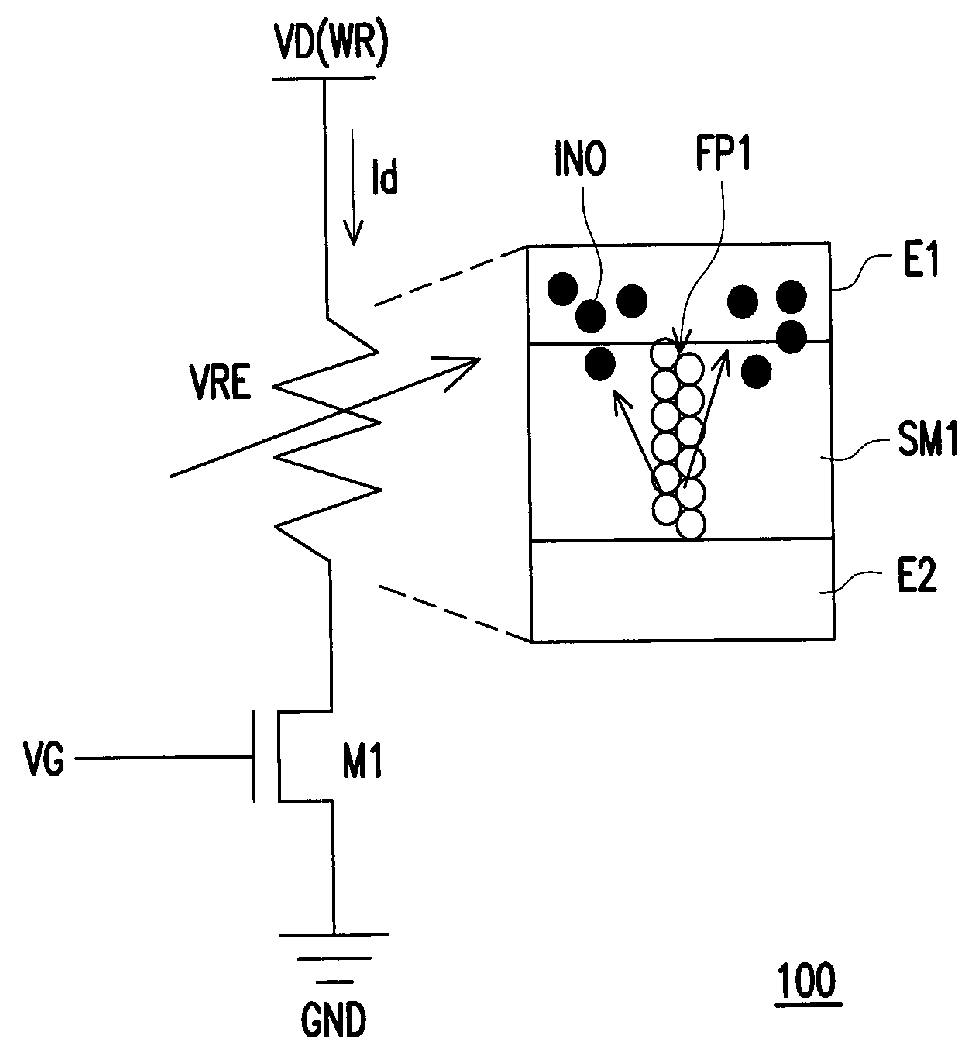
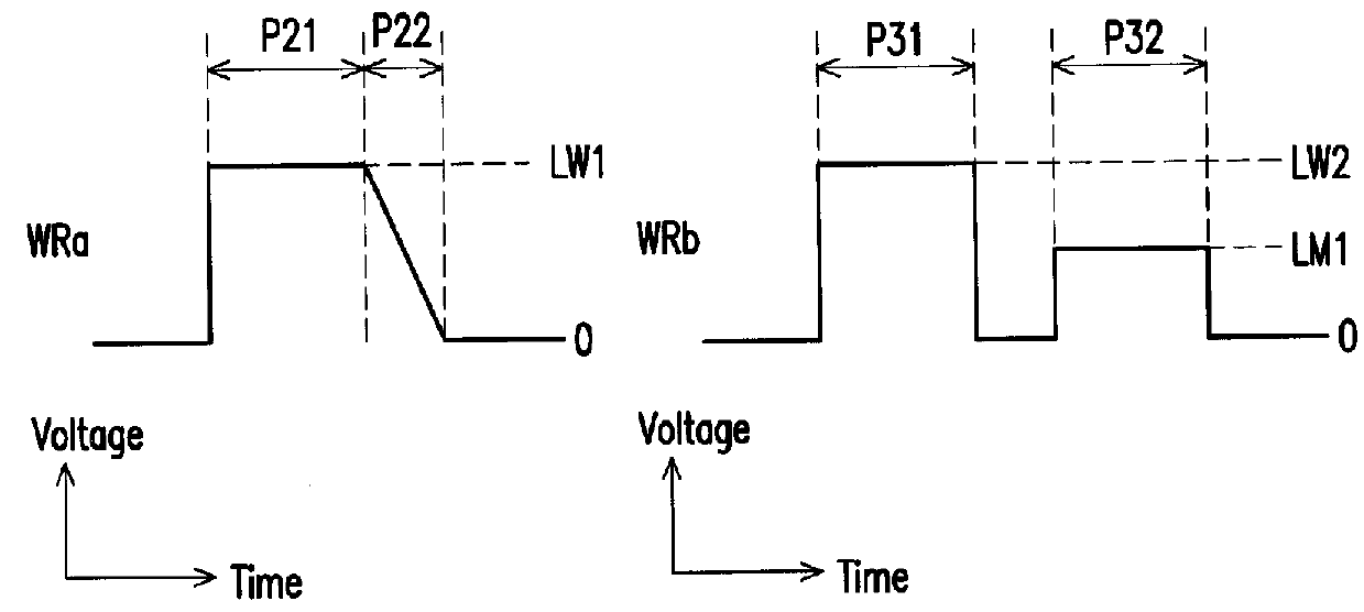
[0021]FIG. 2 is a schematic diagram illustrating a driving waveform of a writing signal according to the invention. Referring to FIG. 1 and FIG. 2, in which the same or similar elements are indicated by the same or similar reference numbers. In the present embodiment, a writing signal WRa is configured to set the variable impedance element VRE. That is, when the transistor M1 is turned-on, the writing signal WRa is provided to the variable impedance element VRE to set an impedance of the variable impedance element VRE.

[0022]In a period P21 (corresponding to a first period), the writing signal WRa is set to a writing voltage level LW1 (corresponding to a first writing voltage level), so as to trigger the oxygen ions INO in the switching medium SM1 to start moving and thereby form the filament path FP1 in the switching medium VRE. Next, in a period P22 (corresponding to a second period), the writing signal WRa is set to be gradually decreased from the writing voltage level LW1 to the ...

second embodiment

[0025]FIG. 3 is a schematic diagram illustrating a driving waveform of a writing signal according to the invention. Referring to FIG. 1 and FIG. 3, in which the same or similar elements are indicated by the same or similar reference numbers. In the present embodiment, a writing signal WRb is also configured to set the variable impedance element VRE. That is, when the transistor M1 is turned-on, the writing signal WRb is provided to the variable impedance element VRE to set the impedance of the variable impedance element VRE.

[0026]In a period P31 (corresponding to the first period), the writing signal WRb is set to a writing voltage level LW2 (corresponding to the first writing voltage level), namely, a pulse with the voltage level being the writing voltage level LW2 is formed, so as to trigger the oxygen ions INO in the switching medium SM1 to start moving and thereby form the filament path in the switching medium VRE. Next, in a period P32 (corresponding to the second period), the ...

third embodiment

[0034]FIG. 5 is a schematic diagram illustrating a driving waveform of a writing signal according to the invention. Referring to FIG. 1, FIG. 3 and FIG. 5, in which the same or similar elements are indicated by the same or similar reference numbers. In the present embodiment, a writing signal WRc includes a period P51 (corresponding to the first period), a period P52 (corresponding to the second period), periods P53, P55 and P57 (corresponding to a plurality of third periods), periods P54, P56 and P58 (corresponding to a plurality of fourth periods), and includes four read time points 510, 520, 530 and 540. Among them, two adjacent periods may considered as one writing set (e.g., SET1 to SET4), and actions of each writing set may refer to FIG. 3, which are not repeated hereinafter.

[0035]In the periods P51, P53, P55 and P57 (corresponding to the first period and the third periods), the writing signal WRc is set to voltage levels LW51 and LW52 to LW54 (corresponding to the first writi...


PUM


Abstract

An operation method of a resistive random access memory (RRAM) cell is provided, wherein the RRAM cell includes a variable impedance element and a switch element connected in series. The operation method includes the following steps. When the switch element is turned-on, a writing signal is provided to the variable impedance element to set an impedance of the variable impedance element. In a first period, the writing signal is set to a first writing voltage level to transmit a first electrical energy to the variable impedance element. In a second period, a second electrical energy is transmitted to the variable impedance element by the writing signal. The second period is subsequent to the first period, the first electrical energy and the second electrical energy are greater than zero, and the second electrical energy is smaller than the first electrical energy.

Description

BACKGROUND OF THE INVENTION[0001]1. Field of the Invention[0002]The invention relates to an operation method, and more particularly, relates to an operation method of a resistive random access memory cell.[0003]2. Description of Related Art[0004]Non-volatile memory is characterized by maintaining the stored data even when the power is off, and has thus become a memory element required in many electronic products for maintaining normal operations. Currently, a resistive random access memory (RRAM) is a non-volatile memory under positive developments in the industry, which has advantages including low writing operation voltage, short writing erase time, long memorizing time, non-destructive read, multi-state memory, simple structure, smaller required area and so on, and also has great potential for future applications in the fields of personal computers and electronic equipments.[0005]However, various issues still need to be solved for the resistive random access memory, such as the i...

Claims


Application Information

Patent Timeline
IPC IPC(8): G11C13/00
CPCG11C2013/0092G11C13/0069G11C13/0007G11C13/0064G11C2213/32G11C2213/79
Inventor HO, CHIA-HUALIAO, SHAO-CHINGWANG, PING-KUNLIN, MENG-HUNG
Owner WINBOND ELECTRONICS CORP
Why Eureka
Try Eureka