Photoelectron fingerprint identifying apparatus

Inactive Publication Date: 2016-03-03
GINGY TECH
View PDF4 Cites 7 Cited by
  • Summary
  • Abstract
  • Description
  • Claims
  • Application Information

AI Technical Summary

Benefits of technology

[0010]In order to overcome the aforementioned deficiency associated with the conventional fingerprint sensors, the present disclosure provides a ph

Problems solved by technology

However, their manufacturing cost and durability still remain to be desired.
Furthermore, since the capacitive sensors themselves are exposed semiconductor dies, subjecting to surface erosion and static charges arising out of the sweat and chemicals of the finger.
Therefore, the durability and the shelf life of the capacitive sensors may be highly questionable.
To solve the above problem, additional sapphire substrates may be laminated onto the surface of the capacitive sensors, which un

Method used


Image

  • Photoelectron fingerprint identifying apparatus
  • Photoelectron fingerprint identifying apparatus
  • Photoelectron fingerprint identifying apparatus

Examples


Embodiment Construction

[0020]The aforementioned and other technical contents, features, and efficacies will be shown in the following detail descriptions of a preferred embodiment corresponding with the reference Figures.

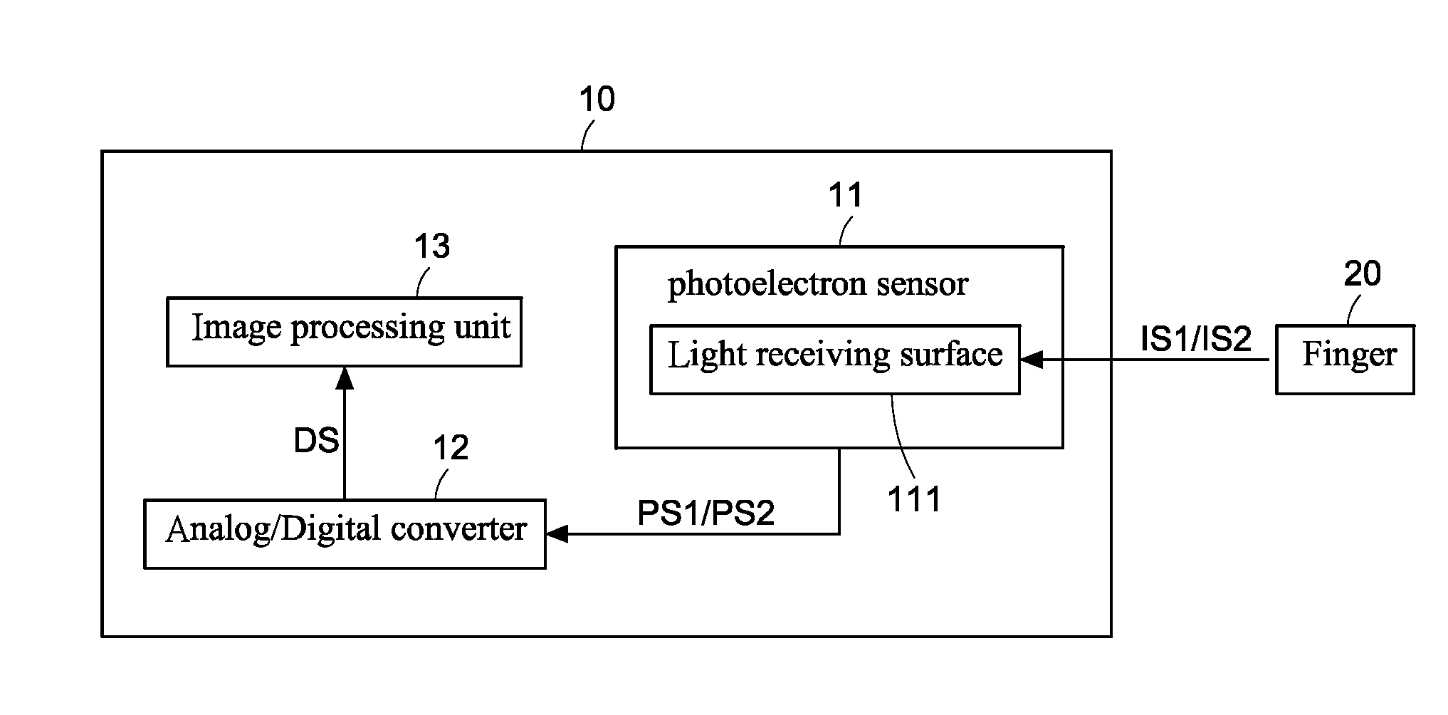
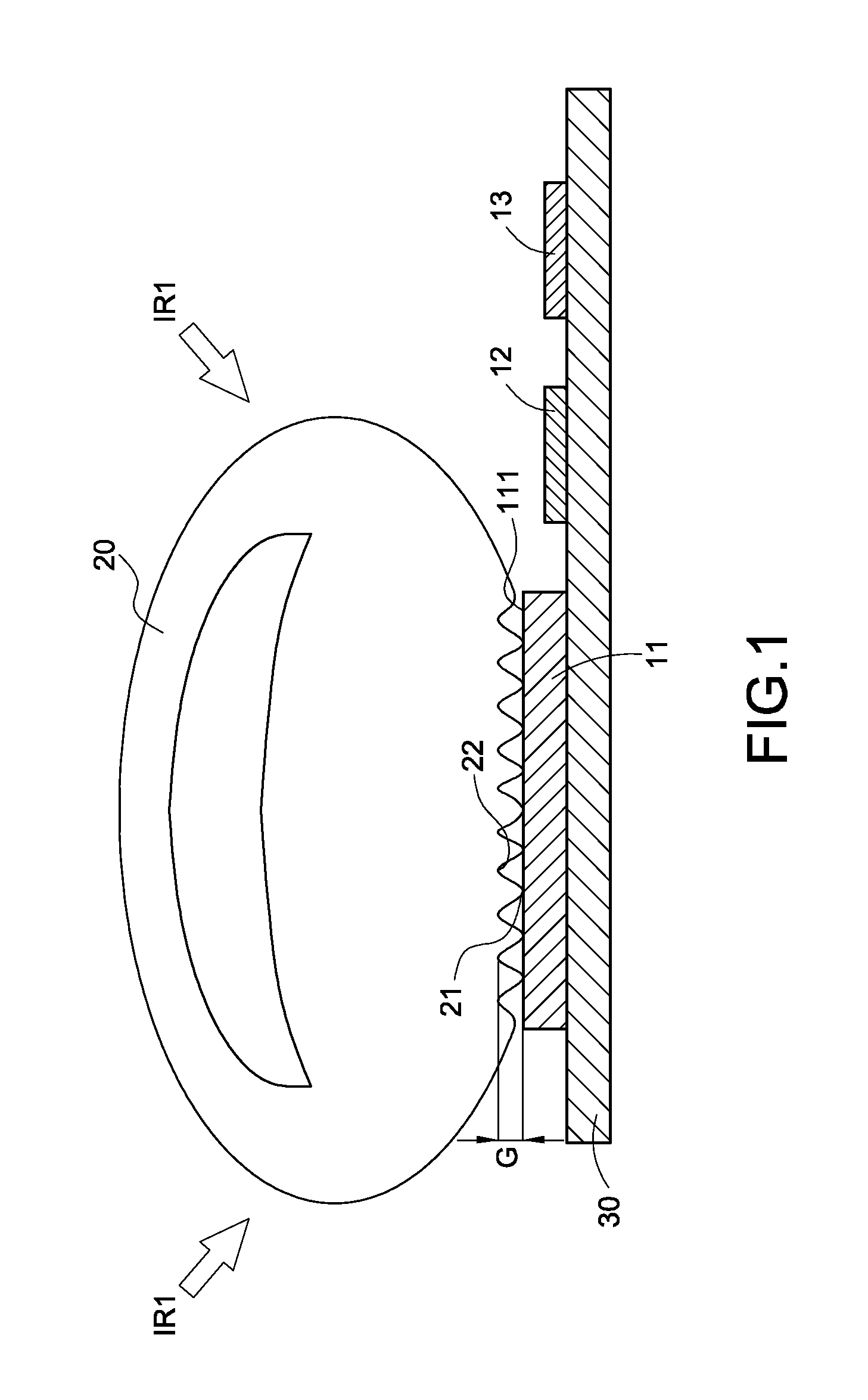
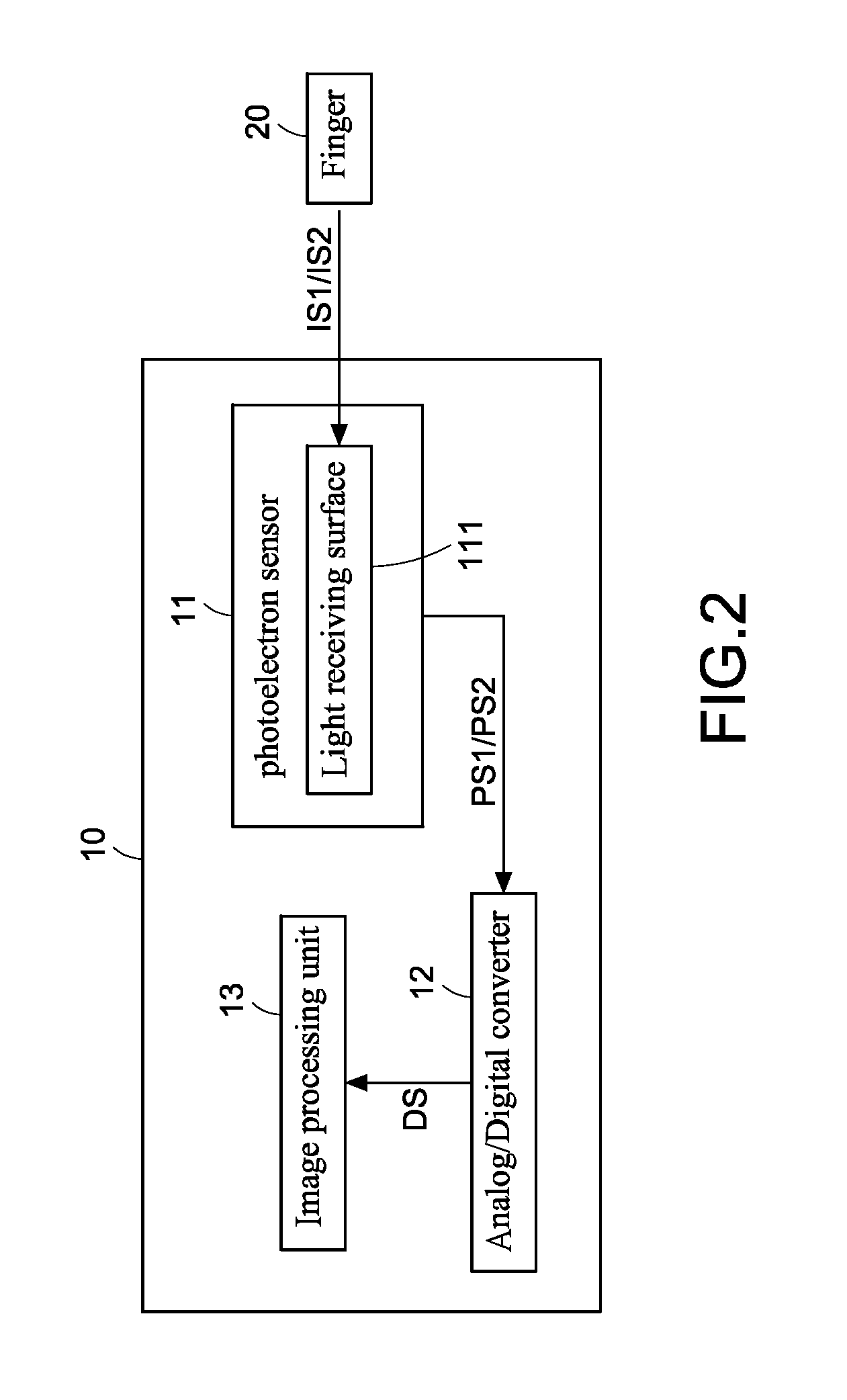
[0021]Please refer to FIGS. 1 and 2 illustrating a simplified block diagram and a structural diagram of a photoelectron fingerprint identifying apparatus 10 according to one embodiment of the present disclosure, respectively. The photoelectron fingerprint identifying apparatus 10 may include a photoelectron sensor 11, an analog / digital (A / D) converter 12, and an image processing unit 13. The photoelectron sensor 11 may include a light receiving surface 111 on which a finger 20 is placed. The A / D converter 12 may be electrically coupled to the photoelectron sensor 11. The image processing unit 13 may be electrically coupled to the A / D converter 12. In one implementation, a circuit board 30 may be provided to have the photoelectron sensor 11, the A / D converter 12, and the image processing u...


PUM


Abstract

A photoelectron fingerprint identifying apparatus is disclosed. The disclosed photoelectron fingerprint identifying apparatus may include a photoelectron sensor having a light receiving surface on which a finger is placed, wherein the photoelectron sensor receives an optical intensity signal associated with an invisible light penetrating the finger before converting the optical intensity signal to a photocurrent signal, an analog/digital converter electrically coupled to the photoelectron sensor for receiving the photocurrent signal, wherein the analog/digital converter converts the photocurrent signal to a digital signal, and an image processing unit electrically coupled to the analog/digital converter for receiving the digital signal before outputting an fingerprint pattern based on the digital signal.

Description

CROSS-REFERENCE TO RELATED APPLICATIONS[0001]This non-provisional application claims priority under 35 U.S.C. §119(a) on Patent Application No(s). 103129359 filed in Taiwan, R.O.C. on Aug. 26, 2014, the entire contents of which are hereby incorporated by reference.BACKGROUND[0002]1. Technical Field[0003]The present disclosure relates to a fingerprint identifying apparatus, in particular, to a photoelectron fingerprint identifying apparatus.[0004]2. Description of Related Art[0005]Fingerprint recognition, as the name suggests, employs the uniqueness of fingerprint for identifying purpose. One typical fingerprint identifying apparatus generally include a fingerprint sensor for capturing a complete fingerprint image and one fingerprint recognition algorithm for processing the fingerprint image such as extracting the characteristics of the fingerprint. Upon a corresponding fingerprint template is generated, the original fingerprint is abandoned before any comparison of the fingerprint p...

Claims


Application Information

Patent Timeline
IPC IPC(8): G06V40/13G06V10/143H04N5/30
CPCH04N5/30G06K2009/0006G06K9/2018G06K9/00013G06V40/1341G06V40/13G06V10/143
Inventor HUNG, CHUN-LANGWU, JEN-CHIEH
Owner GINGY TECH
Why Eureka
Try Eureka