Method for sensing degradation of organic light emitting display

a technology degradation method, which is applied in the field can solve the problems of increasing the manufacturing cost and circuit design area of organic light emitting display, difficult to increase the sensing accuracy, and difficult to uniformly set the sensing current, so as to achieve the effect of increasing the sensing accuracy

Active Publication Date: 2016-03-10
LG DISPLAY CO LTD
View PDF17 Cites 45 Cited by
  • Summary
  • Abstract
  • Description
  • Claims
  • Application Information

AI Technical Summary

Benefits of technology

[0015]Embodiments of the invention provide a method for sensing degradation of an organic light emitting display capable of increasing the sensing accuracy when degradation of an organic element is sensed.

Problems solved by technology

Firstly, the sensing current applied to each organic element has to be uniformly set, so as to accurately sense the degradation of the organic element. For this, the current sources have to be respectively connected to the sensing lines. In this instance, because the number of necessary current sources increases, the manufacturing cost and a circuit design area of the organic light emitting display increase. Furthermore, it is very difficult to uniformly set the sensing currents applied from all of the current sources, and thus it is very difficult to increase the sensing accuracy.
Secondly, the sensing lines may be formed by an independent sensing line structure or a shared sensing line structure depending on a connection structure.
As a result, a degradation speed of the organic element in the related art organic light emitting display having the independent sensing line structure increases, and life span of the related art organic light emitting display decreases.

Method used


Image

  • Method for sensing degradation of organic light emitting display
  • Method for sensing degradation of organic light emitting display
  • Method for sensing degradation of organic light emitting display

Examples


Embodiment Construction

[0034]Reference will now be made in detail to embodiments of the invention, examples of which are illustrated in the accompanying drawings. Wherever possible, the same reference numbers will be used throughout the drawings to refer to the same or like parts. It will be paid attention that detailed description of known arts will be omitted if it is determined that the arts can mislead the embodiments of the invention.

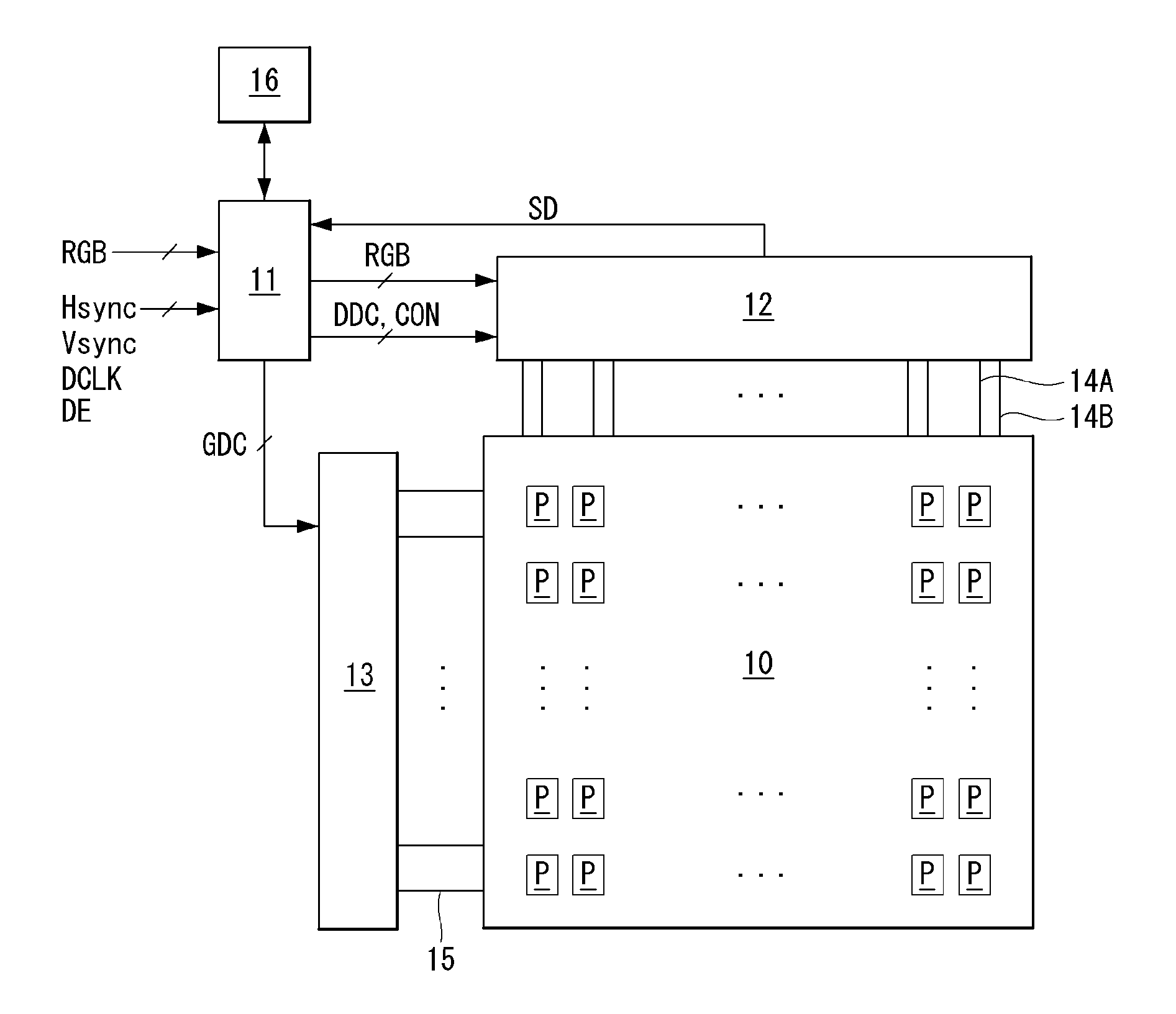
[0035]Configuration of an organic light emitting display, to which a degradation sensing method of the organic light emitting display according to an exemplary embodiment of the invention is applied, is described with reference to FIGS. 1 to 5.

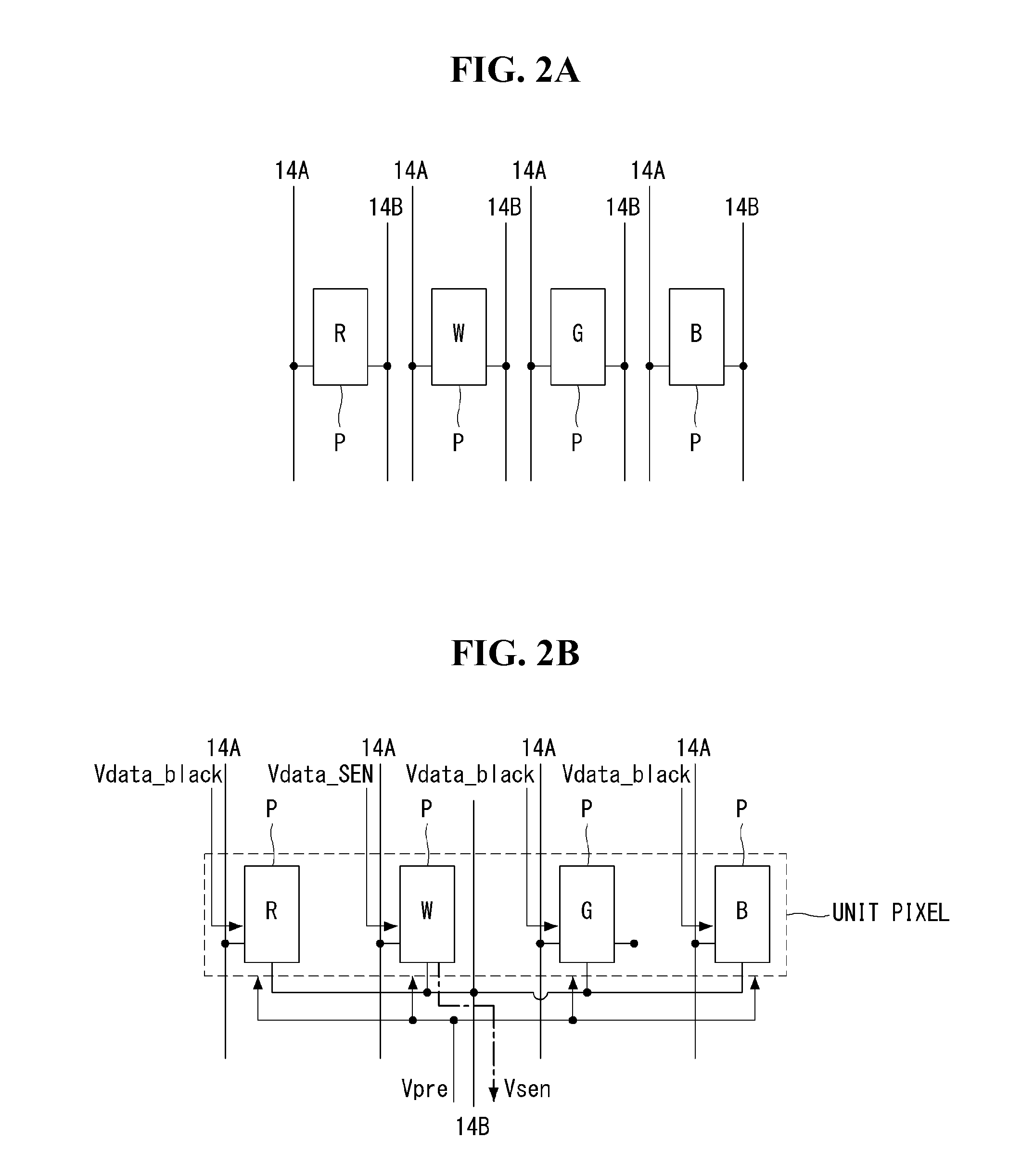
[0036]FIG. 1 shows an organic light emitting display according to an exemplary embodiment of the invention. FIGS. 2A and 2B show an example of the connection between sensing lines and subpixels. FIGS. 3 and 4 show an example of a configuration of a panel array and a data driver integrated circuit (IC).

[0037]As shown in FIGS. 1 to 4...


PUM


Abstract

A method for sensing degradation of an organic light emitting display includes an initialization step for applying a sensing data voltage to a gate node of a driving TFT and applying an initialization voltage to a source node of the driving TFT, a boosting step for floating the gate node and the source node of the driving TFT and applying a drain-to-source current of the driving TFT to an organic element, a sensing step for again applying the initialization voltage to the source node of the driving TFT, setting a gate-to-source voltage of the driving TFT depending on a degradation degree of the organic element, and storing the drain-to-source current of the driving TFT determined by the set gate-to-source voltage in a line capacitor, and a sampling step for outputting a voltage stored in the line capacitor as a sensing voltage.

Description

CROSS-REFERENCE TO RELATED APPLICATION[0001]This application claims the benefit of Korea Patent Application No. 10-2014-0119357 filed on Sep. 05, 2014, which is incorporated herein by reference for all purposes as if fully set forth herein.BACKGROUND OF THE INVENTION[0002]1. Field of the Invention[0003]Embodiments of the invention relate to an organic light emitting display and more particularly to a method for sensing degradation of an organic element of an organic light emitting display.[0004]2. Discussion of the Related Art[0005]An active matrix organic light emitting display includes an organic light emitting diode (hereinafter, referred to as “organic element”) capable of emitting light by itself and has advantages of a fast response time, a high light emitting efficiency, a high luminance, a wide viewing angle, and the like.[0006]The organic element serving as a self-emitting element includes an anode electrode, a cathode electrode, and an organic compound layer formed between...

Claims


Application Information

Patent Timeline
Patent Type & Authority Applications(United States)
IPC IPC(8): G09G3/00G09G3/32
CPCG09G3/006G09G3/3225G09G3/3291G09G2300/0842G09G2330/12G09G2320/043G09G2300/0814G09G3/3233G09G2310/0216G09G2310/027G09G2320/0295G09G2320/045G09G3/32
Inventor KIM, CHANGHEEOH, KILHWANSHIN, HUNKI
Owner LG DISPLAY CO LTD
Why Eureka
Try Eureka