Electronic-component mounting apparatus and electronic-component mounting method

Active Publication Date: 2016-03-17
SHINKAWA CO LTD
View PDF8 Cites 1 Cited by
  • Summary
  • Abstract
  • Description
  • Claims
  • Application Information

AI Technical Summary

Benefits of technology

[0019]The present invention has an advantageous effect of providing an electronic-component mounting

Problems solved by technology

However, using underfill poses a problem that it takes time to fill a liquid resin, as well as a problem that filling a liquid resin

Method used


Image

  • Electronic-component mounting apparatus and electronic-component mounting method
  • Electronic-component mounting apparatus and electronic-component mounting method
  • Electronic-component mounting apparatus and electronic-component mounting method

Examples


Example

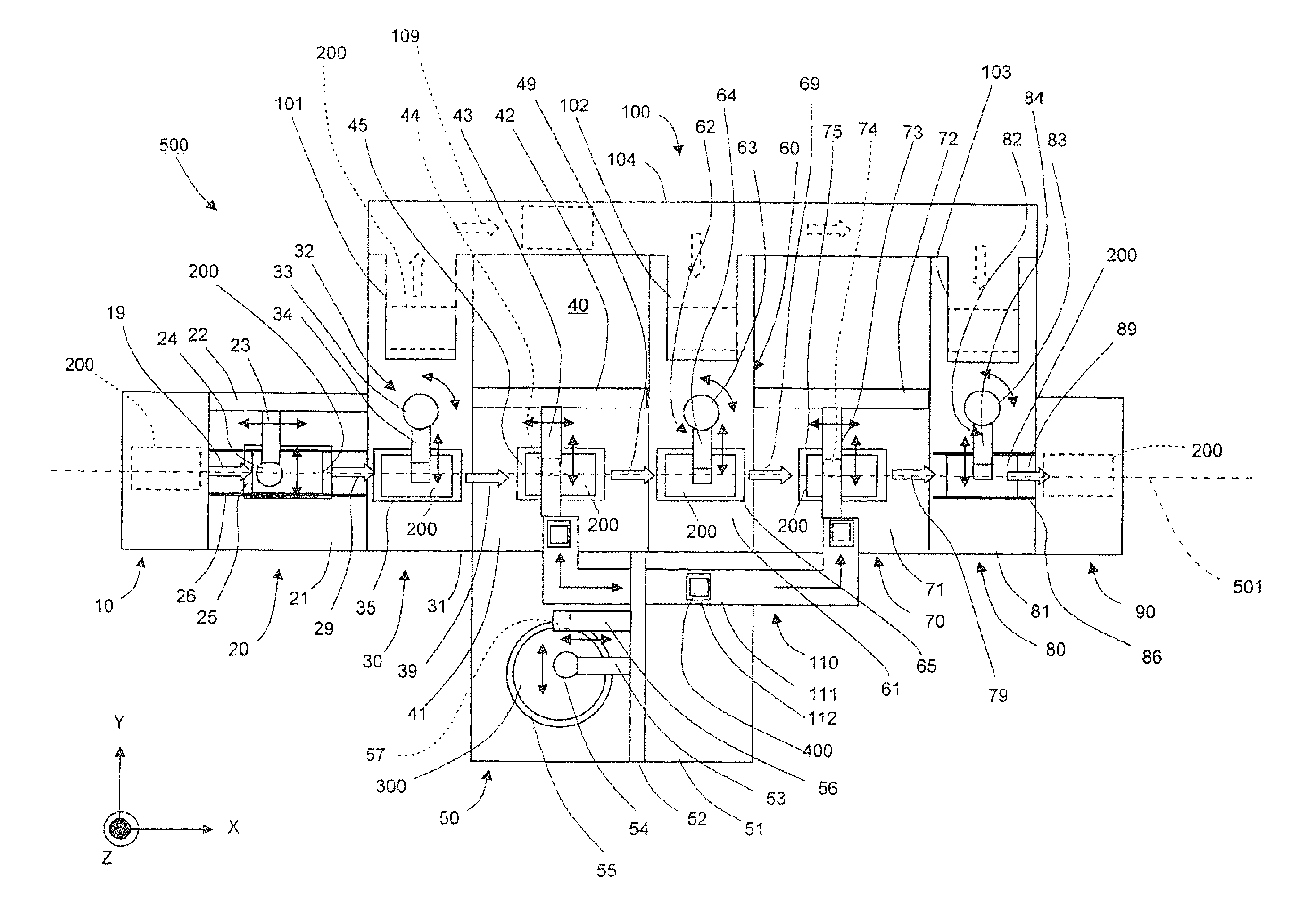
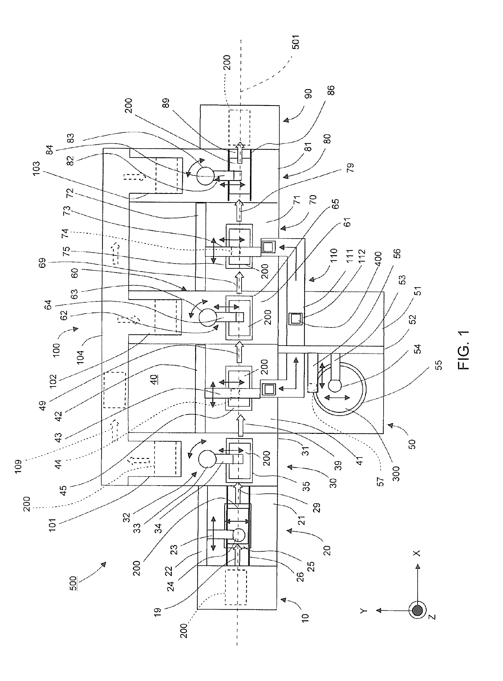
[0043]Hereinafter, embodiments of the present invention applied to a flip chip mounting apparatus will be described with reference to the drawings. As illustrated in FIG. 1, a flip chip mounting apparatus 500 of this embodiment includes a substrate supply block 10, an NCP (non-conductive paste) application block 20, an upstream pre-heating block 30, an upstream mounting block 40, a downstream pre-heating block 60, a downstream mounting block 70, a product discharge block 80, a product storage block 90, a chip pick-up block 50, a chip carrying block 110, and a substrate bypass carrying block 100. Substrates 200 are carried from the substrate supply block 10 toward the product storage block 90 as indicated by white arrows 19, 29, 39, 49, 69, 79, and 89. In this embodiment, the description is given assuming that a carrying direction along which the substrates 200 are carried corresponds to X direction (in a direction along the center line 501), a horizontal direction perpendicular to t...


PUM


Abstract

Provided is a flip chip mounting apparatus for mounting chips (400) to a substrate (200), and the apparatus includes at least one sectionalized mounting stage (45) divided into a heating section (452) and a non-heating section (456), the heating section being for heating a substrate (200) fixed to a front surface of the heating section, the non-heating section not heating the substrate (200) suctioned to a front surface of the non-heating section. With this, it is possible to provide an electronic-component mounting apparatus that is simple and capable of efficiently mounting a large number of electronic components.

Description

CROSS REFERENCE TO RELATED APPLICATIONS[0001]This application is a Continuation of PCT International Application No. PCT / JP2014 / 057293, filed on Mar. 18, 2014, which claims priority under 35 U.S.C §119(a) to Patent Application No. 2013-108658, filed in Japan on May 23, 2013, all of which are hereby expressly incorporated by reference into the present application.TECHNICAL FIELD[0002]The present invention relates to a structure of an electronic-component mounting apparatus, in particular, a structure of a mounting stage of the electronic-component mounting apparatus, as well as to an electronic-component mounting method using such an electronic-component mounting apparatus.BACKGROUND ART[0003]As a method of mounting a chip as an electronic component on a circuit substrate, flip chip mounting in which bump electrodes also referred to as bumps are formed on the chip and the chip is directly mounted to the circuit substrate has become widely employed. The flip chip mounting is a method ...

Claims


Application Information

Patent Timeline
IPC IPC(8): H05K13/04H05K3/30
CPCH05K13/04H05K2203/1105H05K3/30H01L21/67144H01L24/27H01L24/75H01L24/81H01L24/83H01L24/92H01L24/97H01L24/32H01L24/29H01L24/13H01L24/16H01L2224/27318H01L2224/16227H01L2224/16225H01L2224/131H01L2224/32225H01L2224/2919H01L2224/7598H01L2224/75804H01L2224/75822H01L2224/75802H01L2224/75824H01L2224/75744H01L2224/75734H01L2224/75701H01L2224/75702H01L2224/7565H01L2224/75611H01L2224/75501H01L2224/75251H01L2224/75252H01L2224/81815H01L2224/81048H01L2224/83948H01L2224/83986H01L2224/83862H01L2224/8385H01L2224/83048H01L2224/83192H01L2224/97H01L2224/9211H01L2924/00014H01L2924/014H01L2224/81H01L2224/83H05K13/02
Inventor SEYAMA, KOHEI
Owner SHINKAWA CO LTD
Why Eureka
Try Eureka