Overlay mark and method for forming the same

Active Publication Date: 2016-03-31
UNITED MICROELECTRONICS CORP
View PDF0 Cites 10 Cited by
  • Summary
  • Abstract
  • Description
  • Claims
  • Application Information

AI Technical Summary

Benefits of technology

[0013]Since the x-directional and y-directional patterns defined by the first lithography step and those defined by the second lithography step are formed in the same overlay mark, the wafer area required for forming ove

Problems solved by technology

Moreover, because the overlay errors of the two lithography steps are measured with respect to different parts of line

Method used


Image

  • Overlay mark and method for forming the same
  • Overlay mark and method for forming the same

Examples


third embodiment

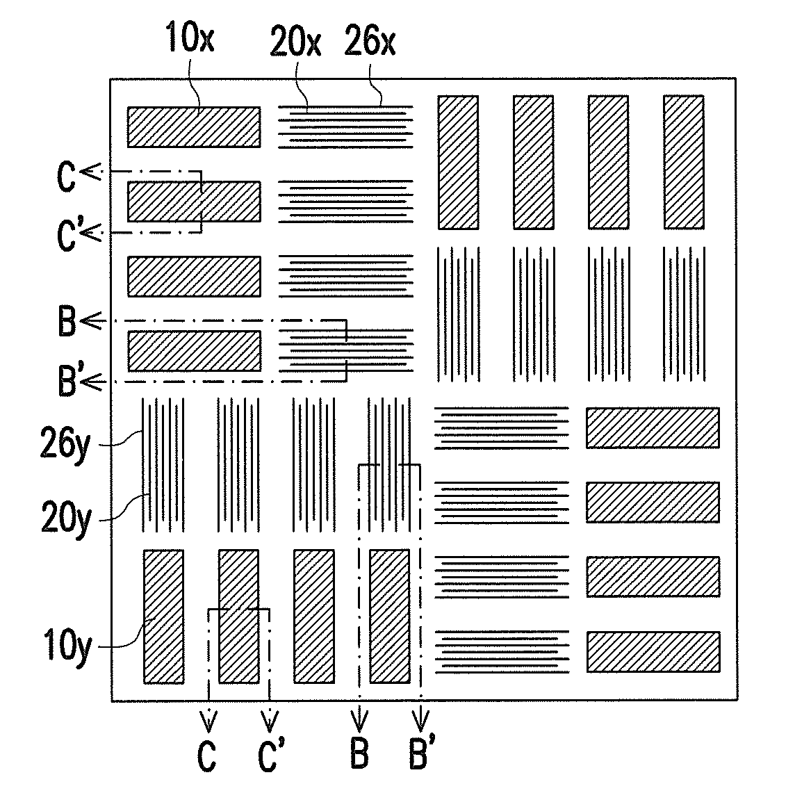
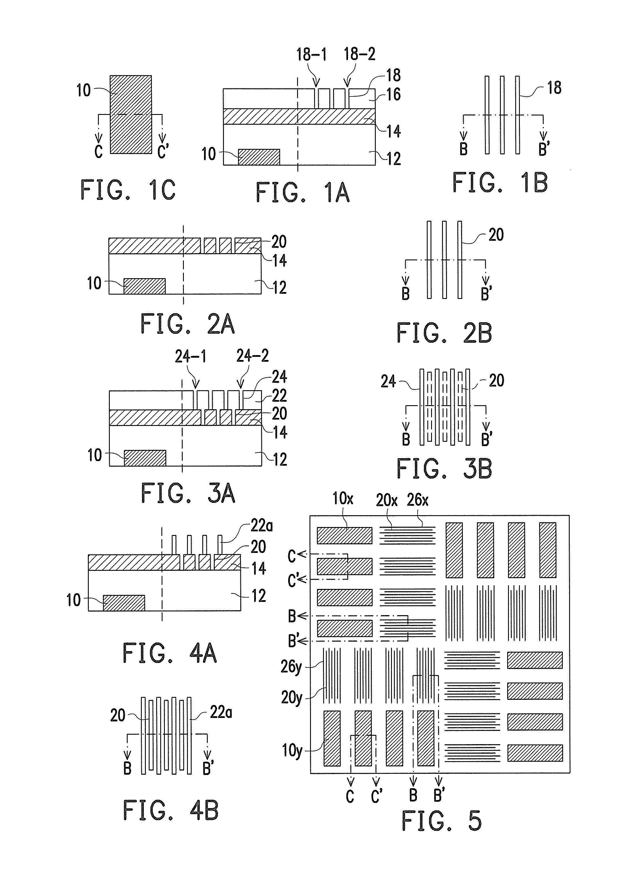
[0022]In addition, for the cases that each group of patterns has a linear shape for each pattern in the group, although there are a specific number of sets of alternately arranged linear patterns defined by the first lithography step and linear patterns defined by the second lithography step arranged in a particular manner in this invention, there may alternatively be a different number of such sets of linear patterns arranged in a different manner.

first embodiment

[0023]FIGS. 1A to 3A, 1B to 3B and 1C schematically illustrate a method for forming an overlay mark for a LELE-type DPL process according to this invention, wherein FIGS. 1A to 3A are cross-sectional views, FIGS. 1B to 3B are top views of linear patterns of the current layer with line B-B′ corresponding to the cross-sectional views, and FIG. 1C is a top view of a linear pattern of the previous layer in the overlay mark with line C-C′ corresponding to the cross-sectional views.

[0024]It is particularly noted that only one linear pattern of the previous layer is illustrated in the figures and described below for both of the x-directional linear pattern and the y-directional linear pattern of the previous layer, since both of them have the same basic shape. Similarly, only one set of parallel linear patterns of the current layer is illustrated in the figures and described below for both of the x-directional linear patterns and the y-directional linear patterns of the current layer defin...

second embodiment

[0030]Though the linear patterns of the current layer defined by the second lithography step are trenches (24) in the second photoresist layer (22), they may alternatively be solid line patterns form from the second photoresist layer, as described in this invention and schematically illustrated in FIGS. 4A and 4B, wherein FIG. 4A and FIG. 4B are a cross-sectional view and a top view, respectively.

[0031]Referring to FIGS. 4A and 4B, in the second lithography step of the DPL process in the second embodiment of this invention, a second photoresist layer is formed in the overlay mark region and the device area (not shown), and then a plurality of parallel solid line patterns 22a (the third x-directional patterns and the third y-directional patterns) of the current layer are formed from the second photoresist layer, simultaneously with the formation of a second part of the patterns of the current layer in the device area (not shown). The solid line patterns 22a defined by the second lith...


PUM


Abstract

An overlay mark applied to a LELE-type double patterning lithography (DPL) process including a first lithography step, a first etching step, a second lithography step and a second etching step in sequence is described. The overlay mark includes a first x-directional pattern and a first y-directional pattern of a previous layer, second x-directional and y-directional patterns of a current layer defined by the first lithography step, and third x-directional and y-directional patterns of the current layer defined by the second lithography step. The second x-directional patterns and the third x-directional patterns are arranged alternately beside the first x-directional pattern. The second y-directional patterns and the third y-directional patterns are arranged alternately beside the first y-directional pattern.

Description

BACKGROUND OF THE INVENTION[0001]1. Field of Invention[0002]This invention relates to an integrated circuit (IC) process, and particularly to an overlay mark applied in a lithography-etching-lithography-etching (LELE)-type double patterning lithography (DPL) process, and a method for forming the overlay mark.[0003]2. Description of Related Art[0004]In order to check the alignment accuracy between patterns of a previous wafer layer and patterns of a current wafer layer that is more important as the linewidth gets smaller, an IC wafer is usually formed with many overlay marks thereon.[0005]Meanwhile, as the linewidth gets smaller, various double patterning processes are utilized to form dense patterns with a pitch smaller than the lithographic resolution. For example, the current layer may be patterned through a process including a first lithography step, a first etching step, a second lithography step and a second etching step in sequence, namely a LELE-type DPL process.[0006]In such...

Claims


Application Information

Patent Timeline
IPC IPC(8): H01L23/544H01L21/027H01L21/033H01L21/311H01L21/66H01L23/532
CPCH01L23/544H01L23/53271H01L21/0274H01L2223/54426H01L21/0332H01L22/20H01L21/31144G03F7/70633H01L2924/0002H01L22/12H01L2924/00
Inventor LIOU, EN-CHIUANKUO, TENG-CHINCHEN, YI-TING
Owner UNITED MICROELECTRONICS CORP
Why Eureka
Try Eureka