Semiconductor laser device

a laser device and semiconductor technology, applied in the direction of semiconductor lasers, lasers, laser construction details, etc., can solve the problems of speckle noise and speck pattern, and achieve the effect of reducing speckle noise, low cost, and easy operation

Active Publication Date: 2016-04-07
MITSUBISHI ELECTRIC CORP
View PDF5 Cites 8 Cited by
  • Summary
  • Abstract
  • Description
  • Claims
  • Application Information

AI Technical Summary

Benefits of technology

[0012]In the semiconductor laser device of the invention, since it is configured that the distance between the opening end of the plurality of openi

Problems solved by technology

As one of characteristics of a semiconductor laser, it is specified that its output light is coherent in phase, in other words, a high coh

Method used


Image

  • Semiconductor laser device
  • Semiconductor laser device
  • Semiconductor laser device

Examples


embodiment 1

[0026]FIG. 1 is a constitution diagram of a semiconductor laser device in accordance with the present embodiment, and shows the semiconductor laser device as seen from the front thereof.

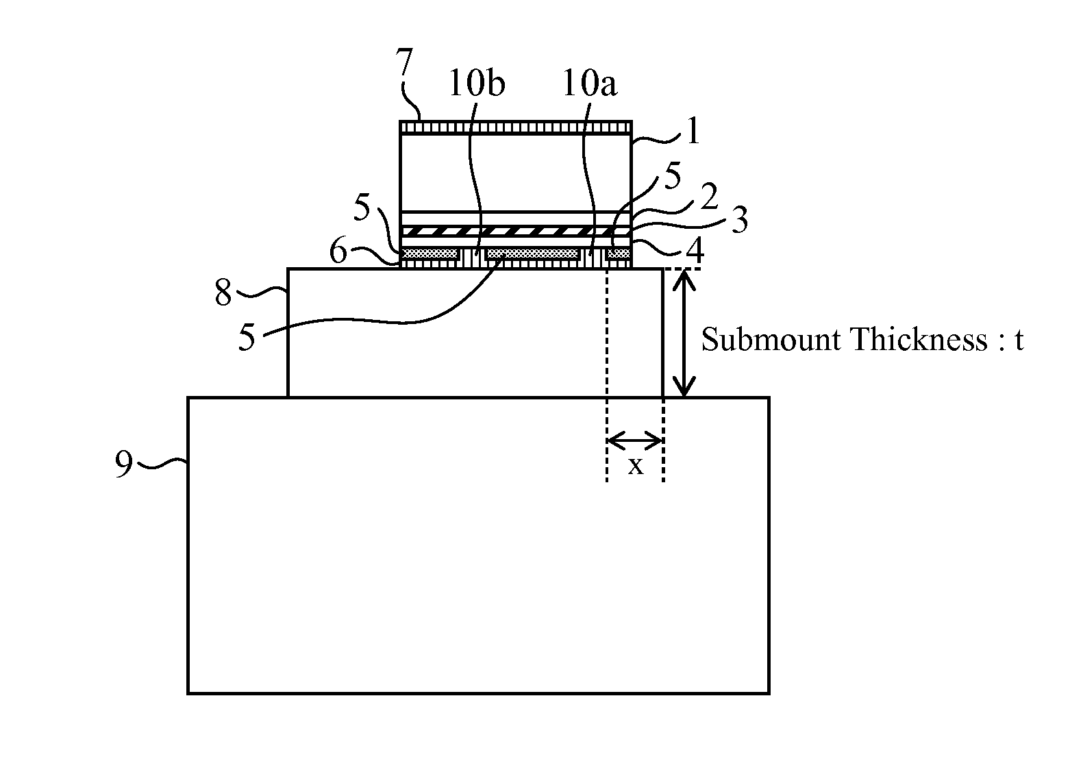
[0027]The illustrated semiconductor laser device includes an n-type GaAs substrate 1, an n-type AlInP cladding layer 2, an active layer 3, a p-type AlInP cladding layer 4, a SiN insulation film 5, a p-side electrode 6, an n-side electrode 7, a submount 8, and a heat sink 9.

[0028]The thickness of the n-type GaAs substrate 1 is about 100 μm; the thickness of the n-type AlInP cladding layer 2 is 1.5 μm; and the active layer 3 has a constitution in which a 10-nm thick undoped GaInP light emitting layer is interposed between two layers of a 200-μm thick undoped AlGaInP optical guide layer, and forms a quantum well. The thickness of the p-type AlInP cladding layer 4 is 1.0 μm; the thickness of the SiN insulation film 5 is 10 nm; the p-side electrode 6 is about 2 μm in thickness; and the n-side electrode 7 ...

embodiment 2

[0050]FIG. 7 is a constitution diagram of a semiconductor laser device in Embodiment 2 as seen from the front thereof. The illustrated semiconductor laser device includes an n-type GaAs substrate 1, an n-type AlInP cladding layer 2, an active layer 3, a p-type AlInP cladding layer 4, a SiN insulation film 5, a p-side electrode 6, an n-side electrode 7, a submount 8, and a heat sink 9. The constituent elements are the same as those of Embodiment 1; however, a positional relationship among the laser element, submount 8, and heat sink 9 is different.

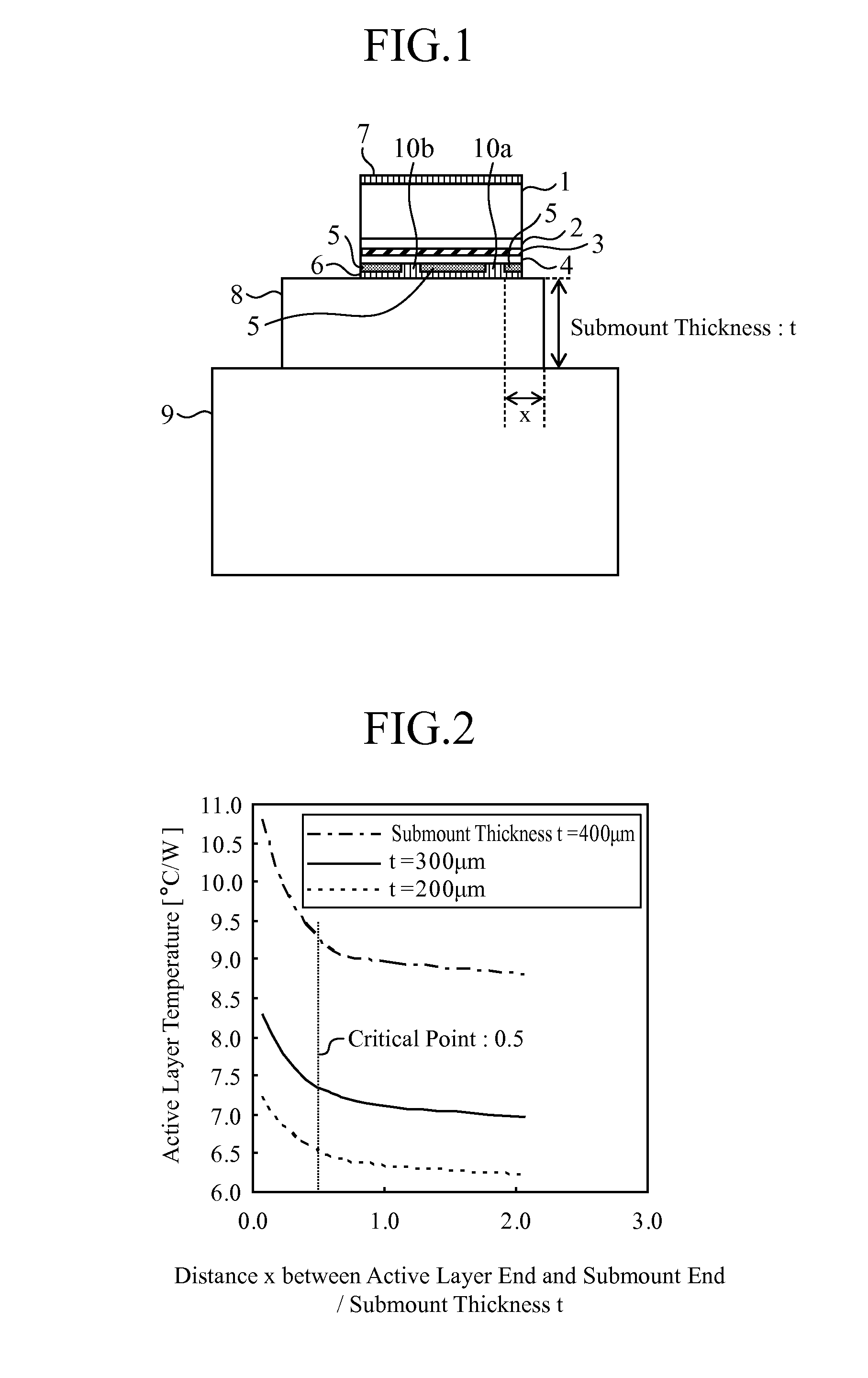
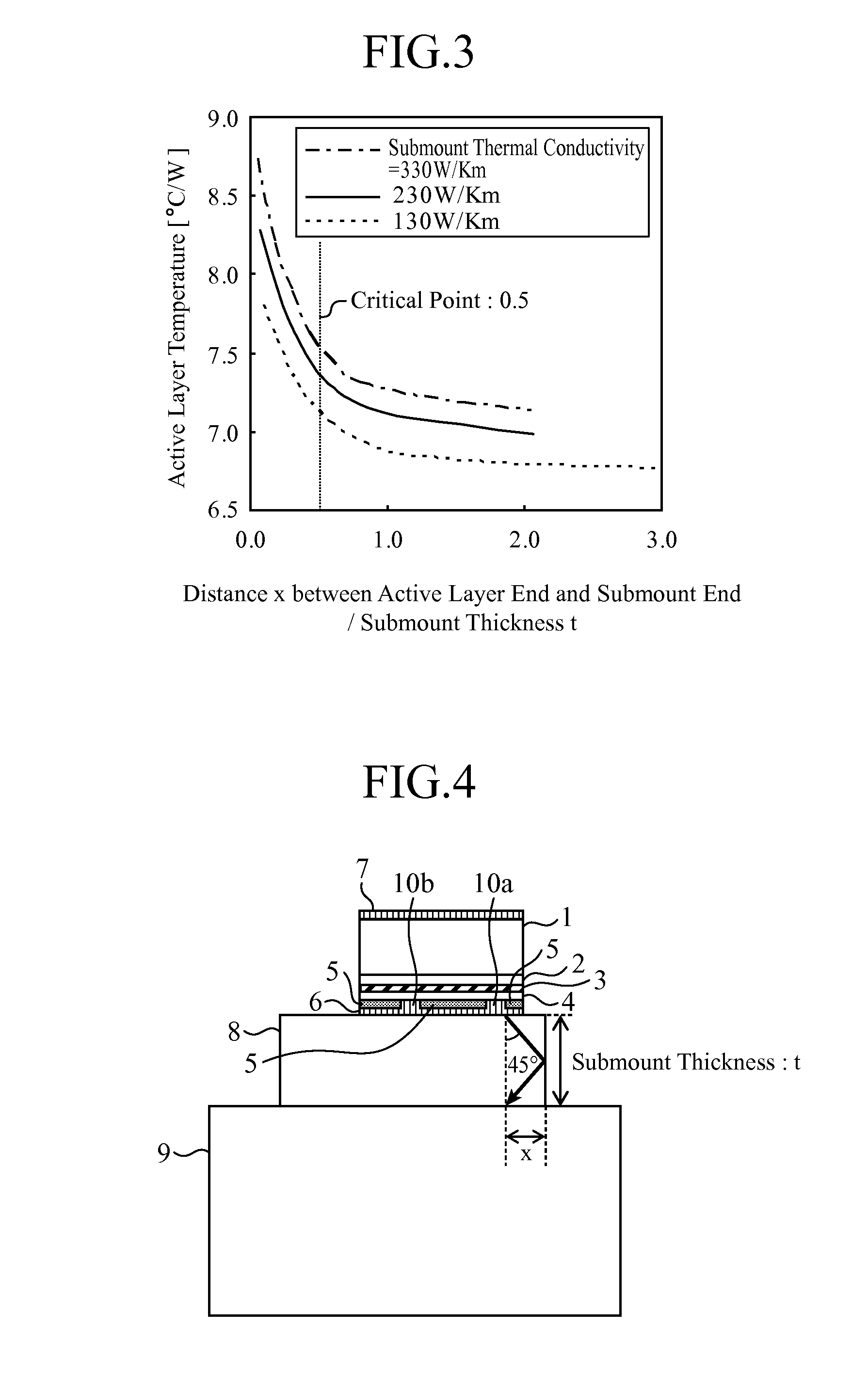
[0051]Here, as shown in FIG. 7, a distance between the right end of the first opening 10a which is one of the two openings, and the right end of the heat sink 9 is referred to as x, and a submount thickness is referred to as t. By application of a thermal simulation with a three-dimensional finite element method to the above structure, determined were the temperatures of the active layer (which is referred to as an active layer 3a) on the f...


PUM


Abstract

In at least one opening of a plurality of openings 10a and 10b, the following inequality is satisfied:
x≦½·t·(kx/ky)
where x represents a minimum distance in a horizontal direction between an end of the one opening and an end of a submount 8, and t represents a thickness of the submount, and
    • in at least one of the other openings different from the one opening, the following inequality is satisfied:
x>½·t·(kx/ky)

Description

TECHNICAL FIELD[0001]The present invention relates to a semiconductor laser device for use in a light source of a projector device, or the like.BACKGROUND ART[0002]A device for displaying a color image such as a projector device or a projection TV requires light sources of three colors of R (red), G (green), and B (blue) as light sources. There is a case in which a semiconductor laser element with a high luminous efficiency is used as the light source. As one of characteristics of a semiconductor laser, it is specified that its output light is coherent in phase, in other words, a high coherence; however, due to this, there arises a problem of appearance of a speckle pattern on a projected surface, a so-called speckle noise.[0003]Thus, as one method of reducing the speckle noise, a means is adopted that a plurality of wavelengths are mixed to reduce the coherence.[0004]Conventionally, as such a device for oscillating the plurality of wavelengths at the same time to reduce the speckle...

Claims


Application Information

Patent Timeline
IPC IPC(8): H01S5/022H01S5/323H01S5/32H01S5/024H01S5/023
CPCH01S5/02236H01S5/3214H01S5/32316H01S5/02469H01S5/024H01S5/0234H01S5/023H01S5/0233H01S5/0235H01S5/4031H01S5/0237H01S5/02476H01S5/022H01S5/06817
Inventor KURAMOTO, KYOSUKEYANAGISAWA, TAKAYUKI
Owner MITSUBISHI ELECTRIC CORP
Why Eureka
Try Eureka