Operating method and device for irradiating a substrate
a technology of irradiation method and substrate, which is applied in the direction of furnace type, furnace type, hearth type furnace, etc., can solve the problems of substrate damage and negative impact on productivity, and achieve the effect of simple and fast retrofitting of the unit and simple and economical operation of the uni
- Summary
- Abstract
- Description
- Claims
- Application Information
AI Technical Summary
Benefits of technology
Problems solved by technology
Method used
Image
Examples
example 1
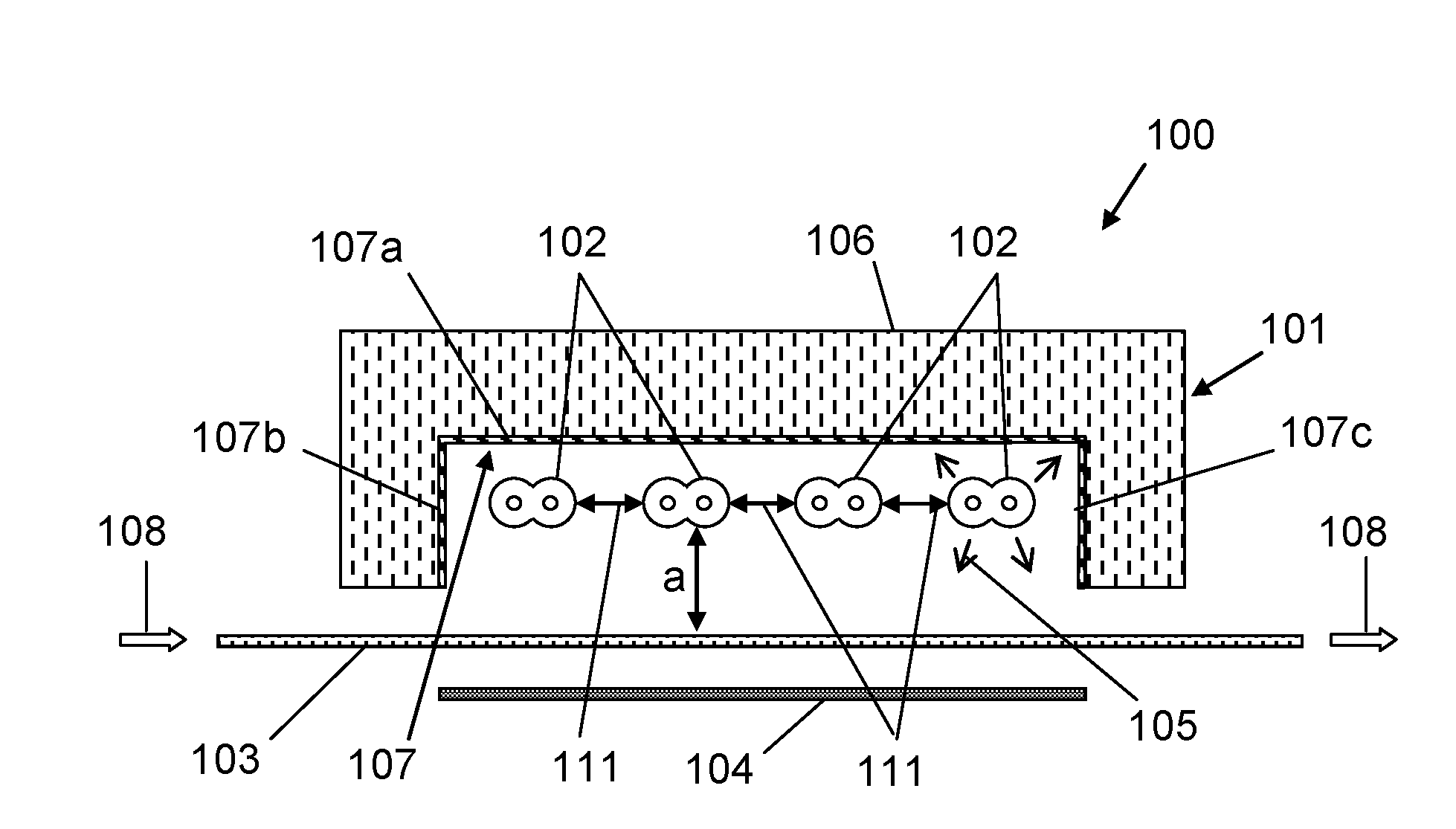
[0081]The irradiating device comprises four infrared emitters having a total of eight filaments. Each infrared emitter is designed for a nominal voltage of 230 V, a nominal output power of 2620 W at a nominal temperature of 2600° C. The heated filament length is 350 mm.
[0082]At a specified total irradiation intensity of 5850 W, varying the operating voltage Ui and the number of illuminated emitters n makes it possible to change the radiation spectrum, as shown in Table 1. Here, Pi is the operating output power of a filament, is Ptotal is the total irradiation output power, T is the filament temperature, λmax is the wavelength of the main emission line, and Pi / Pnominal is the ratio in percent of the individual operating output power to the nominal output power.
TABLE 1UiPiPtotalTλmaxPi / PnominalVariant[V][W]n[W][° C.][nm][%]1100710856801830137527.121601480459202250115056.5325030002600027001000114.541901930357902415108073.7
[0083]As Table 1 shows, a nearly constant total irradiation outp...
example 2
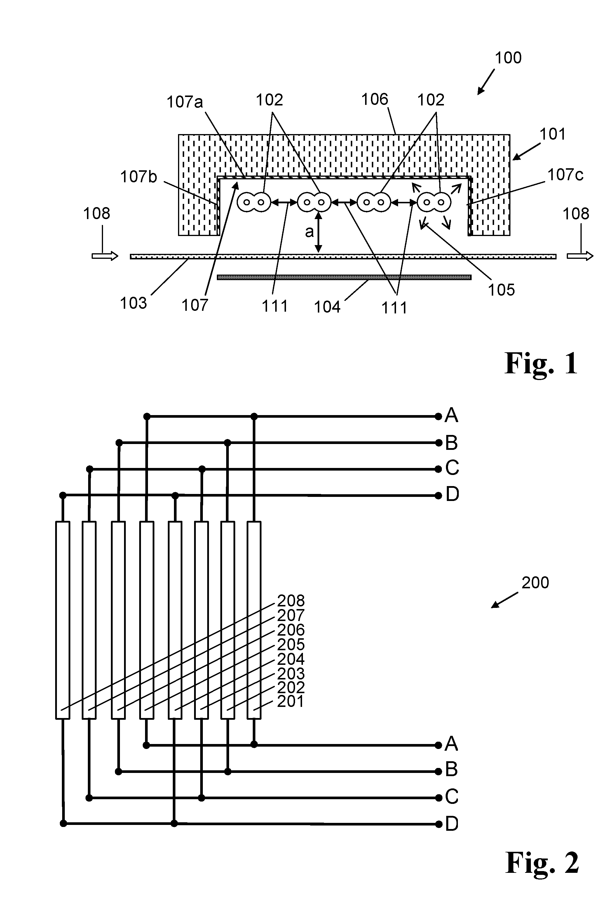
[0085]An irradiating device for drying and sintering inks comprises an infrared emitter module having 12 twin tube infrared emitters each having 2 filaments. The total number of filaments is 24. As Table 3 below shows, by different switching of the filaments, different color temperatures can be achieved with the emitter module at an approximately constant output power density of 120 kW / m2.
TABLE 3Output powerdensityUiTemitter fieldVariant[V]n[° C.][kW / m2]12308260012421601222501113110221910115
[0086]As the substrate, both a plastic film made of polyethylene naphthalate (PEN) and also a plastic film made of polyethylene terephthalate (PET) are used, each with a film thickness of 100 μm. The plastic films were printed with an inkjet printer (Dimatix DMP283; Dropspace 25 / 30 μm) having silver-containing ink. As ink a dispersion of silver nanoparticles (20 weight percent) in organic solvents is used (Suntronic® Jet Silver U 5603).
[0087]The printed plastic films were then dried by the irradi...
PUM
 Abstract
Description
Claims
Application Information


