Conductor pattern structure of capacitive touch panel

Inactive Publication Date: 2016-04-28
HYCON TECH
View PDF0 Cites 2 Cited by
  • Summary
  • Abstract
  • Description
  • Claims
  • Application Information

AI Technical Summary

Benefits of technology

The present invention is about a capacitive touch panel that creates an even electrical field. When applied to a double-layered induced structure, the panel includes two capacitive induced layers separated by an insulating material. The layers have conductor assemblies arranged in the same axial direction. The panel also has a number of floating induced cells distributed between the conductive cells. These cells help even out the electrical field and increase the sensing area. In a single-layered induced structure, the panel has two axial conductor assemblies separated by an insulating layer. The conductor assemblies also include floating induced cells. The addition of these floating induced cells improves the sensing range and increases the range of touch sensing area. The technology of floating induced cells can be applied to both single-layered and double-layered induced structures.

Problems solved by technology

However, the defect is to increase the number of conduction lines and complexity of the control circuit.
I347545, although both patents indicate the function to sense users' touch on the touch panel, there are limitations of uneven distribution of the electrical field and sensing area due to the conductive cells in both prior arts.
If the users only touch the center portion of the conductive cell, the conductive cell can not process to sense.
Otherwise, there would be some area where it is not able to process to sense.
Although it has the effect to improve distribution of an electrical field and increase sensitivity, the defect is to increase the number of conduction lines and complexity of the control circuit, causing serious signal interference among the conduction lines.
It is difficult to implement since there are too many conduction lines if the method is applied to a large control panel.

Method used


Image

  • Conductor pattern structure of capacitive touch panel
  • Conductor pattern structure of capacitive touch panel
  • Conductor pattern structure of capacitive touch panel

Examples


first embodiment

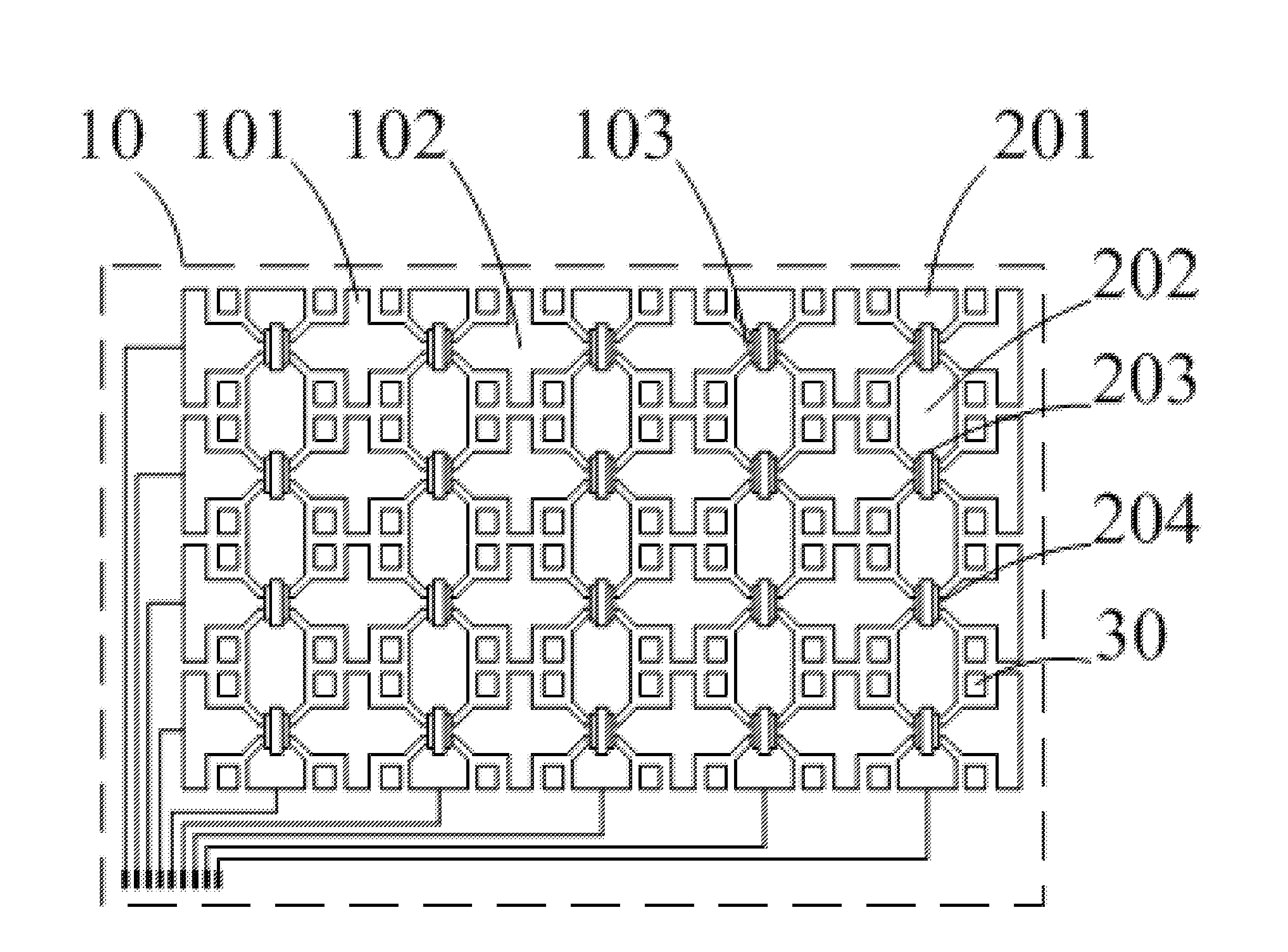
[0033]Please refer to FIG. 4. the present invention is illustrated. It shows a conductor pattern structure of a single-layered induced capacitive touch panel. A capacitive induced layer 10 includes 4 transverse first axial conductor assemblies 101, 5 longitudinal second axial conductor assemblies 201 and 80 floating induced cells 30. Each first axial conductor assembly 101 includes 6 first axial conductive cells 102. Adjacent first axial conductive cells 102 are connected directly by a conduction line 103. Each second axial conductor assembly 201 includes 5 second axial conductive cells 202. Adjacent second axial conductive cells 202 is covered by an insulating material then connected by a conduction line 203 on the surface of the insulating layer 204. Each floating induced cell 30 is placed in a gap between one first axial conductive cell 102 and a second axial conductive cell 202.

[0034]FIG. 5 illustrates a partially enlarged view of two axial conductive cells and floating induced ...

second embodiment

[0036]Please refer to FIG. 6. the present invention is illustrated. It shows a conductor pattern structure of a single-layered induced capacitive touch panel. The capacitive induced layer 10 includes 4 transverse first axial conductor assemblies 101, 5 longitudinal second axial conductor assemblies 201 and 80 floating induced cells 30. Each first axial conductor assembly 101 includes 5 connected first axial conductive cells 102. Each second axial conductor assembly 201 includes 4 second axial conductive cells 202. Each floating induced cell 30 is placed in the gap between one first axial conductive cell 102 and one second axial conductive cells 202.

[0037]In this embodiment, the way to connect conductive cells is different from that of the first embodiment. The first axial conductor assemblies 101 in this embodiment have box-shaped first axial conductive cells 102 which are directly connected. The cruciform second axial conductive cells 202 in the second axial conductor assemblies 20...

third embodiment

[0038]Please refer to FIG. 7. the present invention is illustrated. It shows a conductor pattern structure of a double-layered induced capacitive touch panel. A first induced layer 10 includes 3 transverse first axial conductor assemblies 101. Each first axial conductor assembly 101 includes 5 first axial conductive cells 102 connected by a conduction line 103 and then formed as an elongated shape. The second induced layer 20 includes 5 second axial conductor assemblies 201 arranged according to a second axial direction. Each second axial conductor assembly 201 includes 3 second axial conductive cells 202 connected by a conduction line 203. The second axial conductive cells 202 have a cruciform shape. An insulation layer is formed by an insulating material and between the first induced layer 10 and the second induced layer 20. Therefore, a capacitive effect is formed. The second induced layer 20 further includes 60 floating induced cells 30. Each floating induced cell 30 between sec...


PUM


Abstract

Disclosed is a conductor pattern structure of a capacitive touch panel. The structure contains two conductor assemblies with different directions, and each conductor assembly includes a number of conductive cells that are interconnected by conduction lines. Conductor assemblies with different directions are separated by an insulating material. An electrical field and induced capacitors are generated between adjacent conductor assemblies with different directions when giving control signals. Then the touched location is detected. The capacitive induced layer structure also contains a number of floating induced cells, distributed among the adjacent conductive cells. The floating induced cells generate new induced capacitors without connecting to any conduction lines and requiring any control signals. Therefore, the structure has advantages of improving the distribution of the electrical field and enlarging the touch sensing area.

Description

FIELD OF THE INVENTION[0001]The present invention relates to a designed structure of a touch panel. More particularly, the present invention relates to a conductor pattern structure of a capacitive touch panel. Touch panels have been applied in large numbers to products of home appliances, communications, electronic information etc., such as wildly commercial Personal Digital Assistant (PDA), every home appliances and gaming input interfaces. With integration of touch panels and displays, it is available for users to use fingers or a stylus to select or input what they want to act according to functional options on a displayed screen of a PDA, a home appliance or a gaming input interface. Thus, it is used as a query tool for public systems so as to provide an operating system which has convenient effects.BACKGROUND OF THE INVENTION[0002]The known touch panel is made by forming a sensing area on one surface of the substrate. Touch control is available in the sensing area by sensing h...

Claims


Application Information

Patent Timeline
IPC IPC(8): G06F3/044
CPCG06F3/044G06F3/0416G06F3/0445G06F3/0446G06F2203/04111G06F3/0412G06F2203/04103
Inventor WANG, HUI-MINWANG, YU-JEN
Owner HYCON TECH
Why Eureka
Try Eureka