
Optical module package and its packaging method

a technology of optical modules and optical modules, applied in the direction of semiconductor/solid-state device manufacturing, semiconductor devices, electrical apparatus, etc., can solve the problems of increasing the difficulty, affecting so as to reduce the difficulty of manufacturing the optical module package and the level of difficulty, avoid the crosstalk effect of light signals, and enhance the performance and application of optical modules

Active Publication Date: 2016-05-05
LINGSEN PRECISION INDS
View PDF2 Cites 12 Cited by
  • Summary
  • Abstract
  • Description
  • Claims
  • Application Information

AI Technical Summary

Benefits of technology

The patent text describes a method of preventing light signals from interfering with each other in an optical module package. This is achieved by creating a cavity in the substrate and positioning a stop wall in the substrate to block the light emitted from the chip. The cover, which is made of a resin, can be adjusted to fit different needs, improving the performance and application of the package while reducing manufacturing costs.

Problems solved by technology

However, the prior art optical module package needs an engagement structure for the mounding of the metal frame, complicating the manufacturing process and increasing the level of difficulty.
Further, the fabrication of this prior art optical module package requires a gluing process to bond the metal frame.
If an excessive amount of glue is applied, a problem of glue overflow can occur.
If the applied amount of glue is insufficient, the metal frame can fall off or move out of place, lowering the light isolation effect.

Method used


Image

  • Optical module package and its packaging method
  • Optical module package and its packaging method
  • Optical module package and its packaging method

Examples


Embodiment Construction

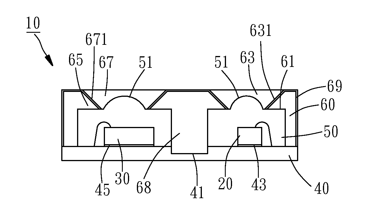
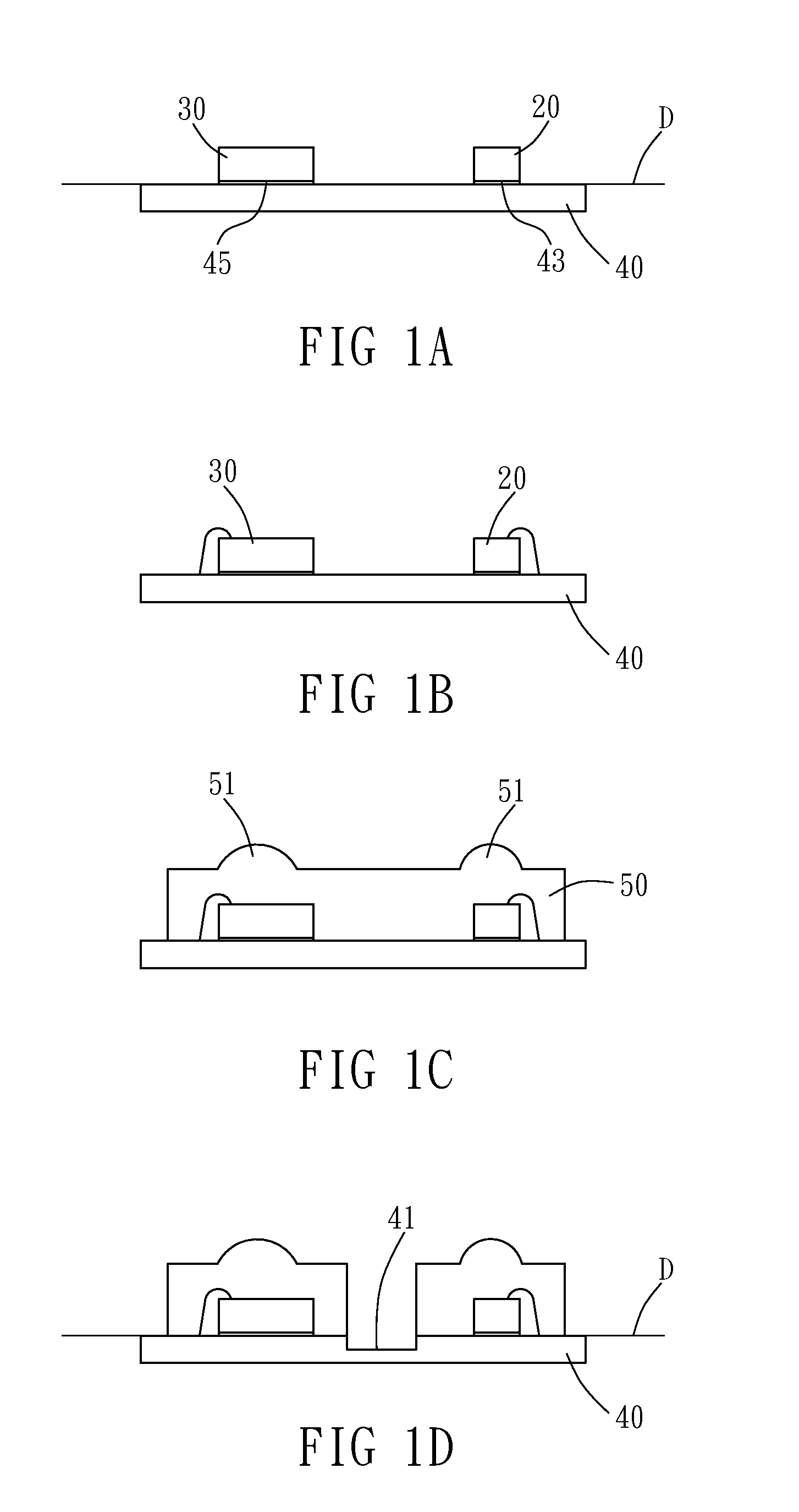
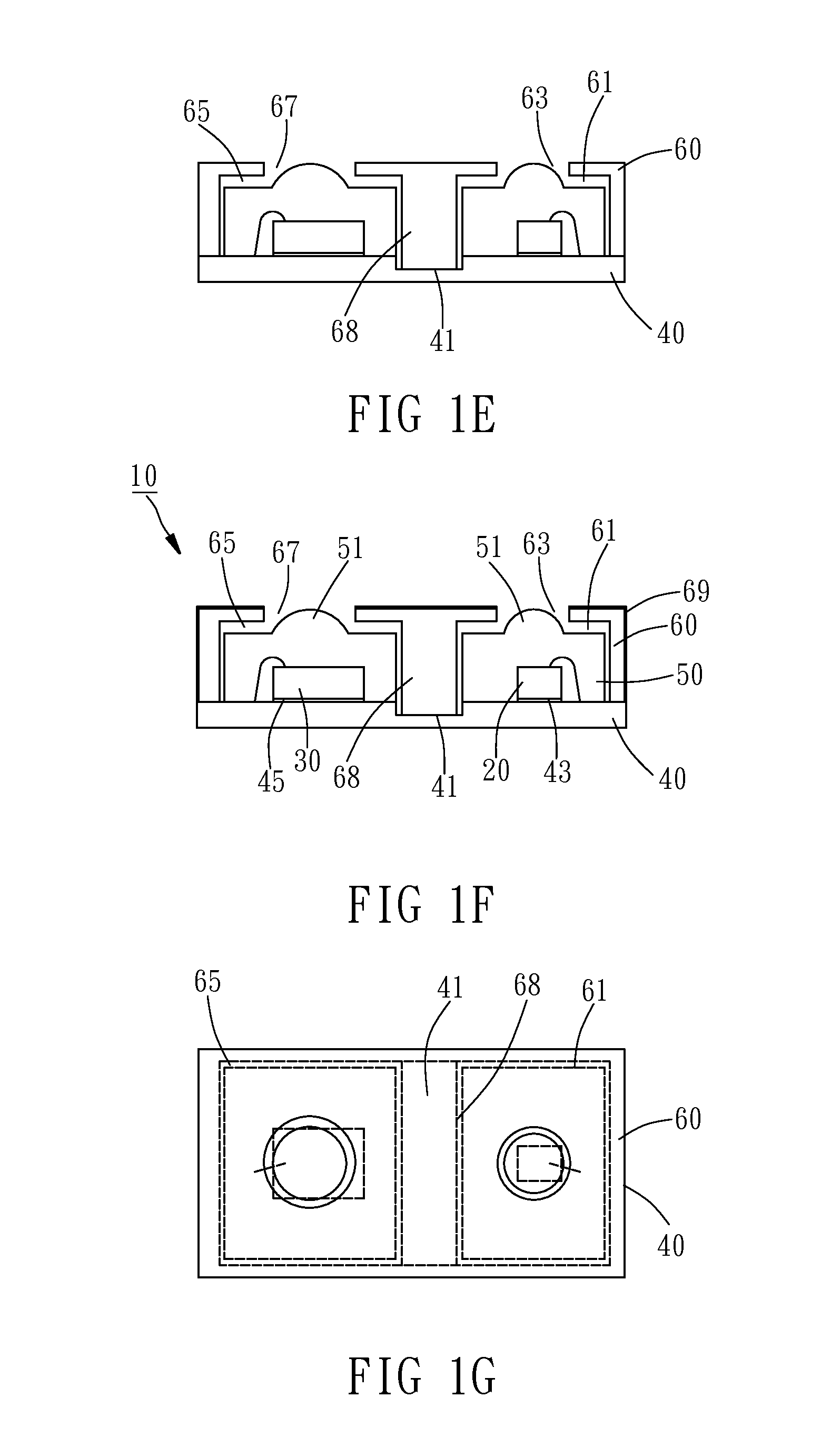
[0030]Referring to FIGS. 1A through 1F, an optical module package 10 in accordance with a first embodiment of the present invention is shown. The fabrication of the optical module package 10 comprises the following steps:

[0031]Step (a): As illustrated in FIGS. 1A and 1B, employ a die bonding process to bond a light-emitting chip 20 and a light-receiving chip 30 to a substrate 40, and then employ a wire bonding process to electrically connect the light-emitting chip 20 and the light-receiving chip 30 to the substrate 40.

[0032]Step (b): As illustrated in FIG. 1C, employ a molding process to mold an encapsulation colloid 50 on the substrate 40 over the light-emitting chip 20 and the light-receiving chip 30. In the molding process, a light guide portion 51 is simultaneously formed in the encapsulation colloid 50. This method not only can simplify the manufacturing process, but also can enhance the light signal transmitting and receiving efficiency.

[0033]Step (c): As illustrated in FIG. ...


PUM


Abstract

An optical module package includes a substrate having a recessed portion, a cover covered on the substrate and defining with the substrate a first chamber and a second chamber therebetween, the cover having a light-emitting hole disposed in communication with the first chamber, a light-receiving hole disposed in communication with the second chamber and a stop wall positioned in the recessed portion to separate the first chamber and the second chamber, a light-emitting chip and a light-receiving chip mounted at the substrate and respectively disposed in the first chamber and the second chamber, and two encapsulation colloids respectively mounted in the first chamber and the second chamber and respectively wrapped about the light-emitting chip and the light-receiving chip. Thus, the optical module package not only can prevent crosstalk but also can greatly reduce the manufacturing cost and the level of difficulty.

Description

BACKGROUND OF THE INVENTION[0001]1. Field of the Invention[0002]The present invention relates to semiconductor packaging technology and more particularly, to an optical module package and its packaging method.[0003]2. Description of the Related Art[0004]In order to prevent the touch panel from being inadvertently triggered or to satisfy power-saving requests, regular handheld electronic devices (such as smart phone, etc.) generally have an optical module mounted therein. When approaching a handheld electronic device of this design to the surface of an object (for example, one's cheek), a light-emitting chip of the optical module will emit light onto the surface of the object, and a light-receiving chip of the optical module will receive the reflected light and convert it into an electronic signal for follow-up processing.[0005]However, in order to avoid crosstalk interference, the optical module package uses an encapsulation colloid to encapsulate the light-emitting chip and the lig...

Claims


Application Information

Patent Timeline
Patent Type & Authority Applications(United States)
IPC IPC(8): H01L31/153H01L31/0203H01L31/0232
CPCH01L31/153H01L31/0203H01L31/02327H01L25/167H01L2924/181H01L2224/92227H01L2224/32225H01L2224/48091H01L2224/48227H01L2224/73265H01L31/173H01L2924/00014H01L2924/00012H01L2924/00
Inventor TU, MING-TELIN, YU-CHEN
Owner LINGSEN PRECISION INDS
Learn More