
Shared global read and write word lines

Active Publication Date: 2016-05-19
QUALCOMM INC
View PDF0 Cites 9 Cited by
  • Summary
  • Abstract
  • Description
  • Claims
  • Application Information

AI Technical Summary

Benefits of technology

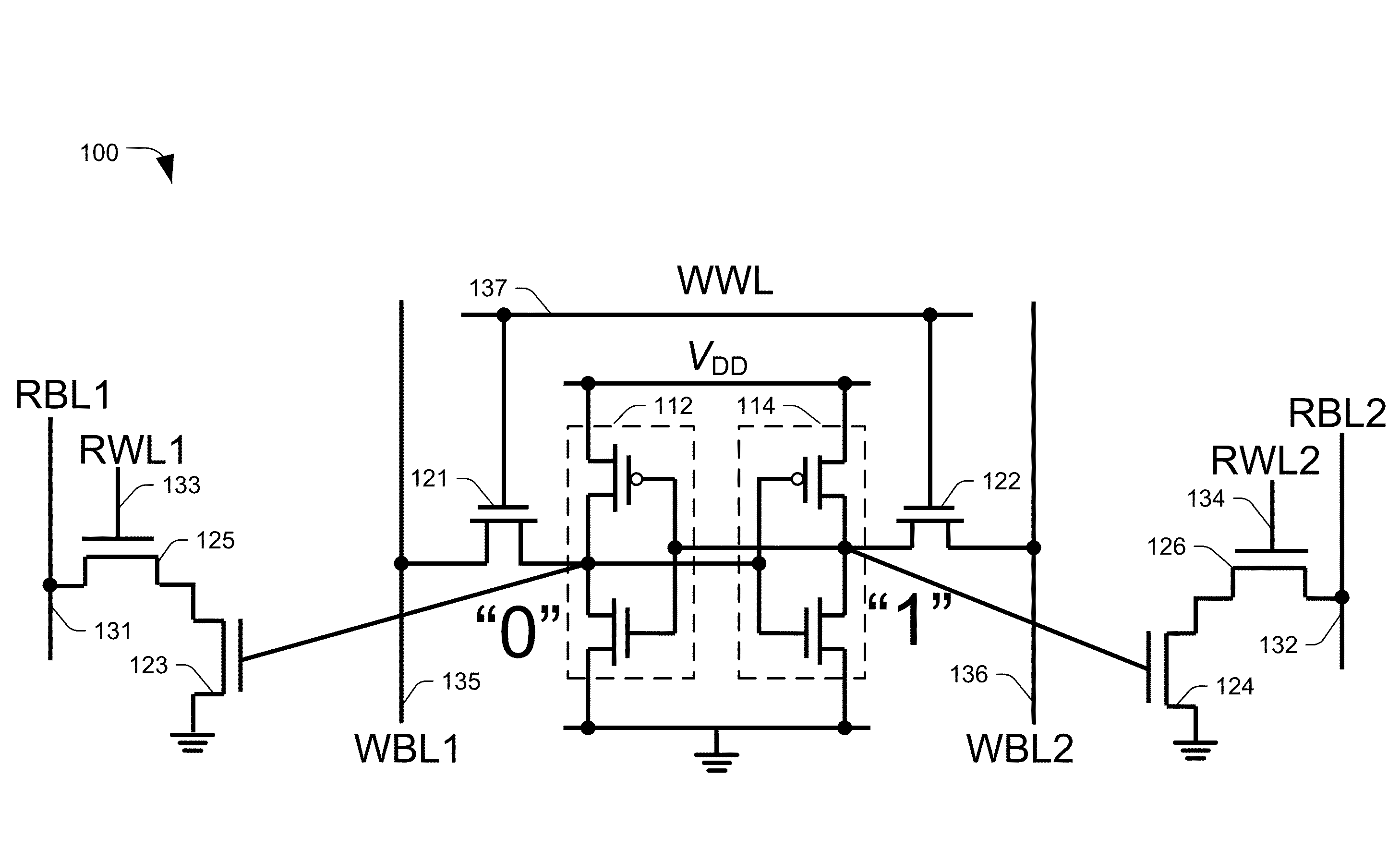
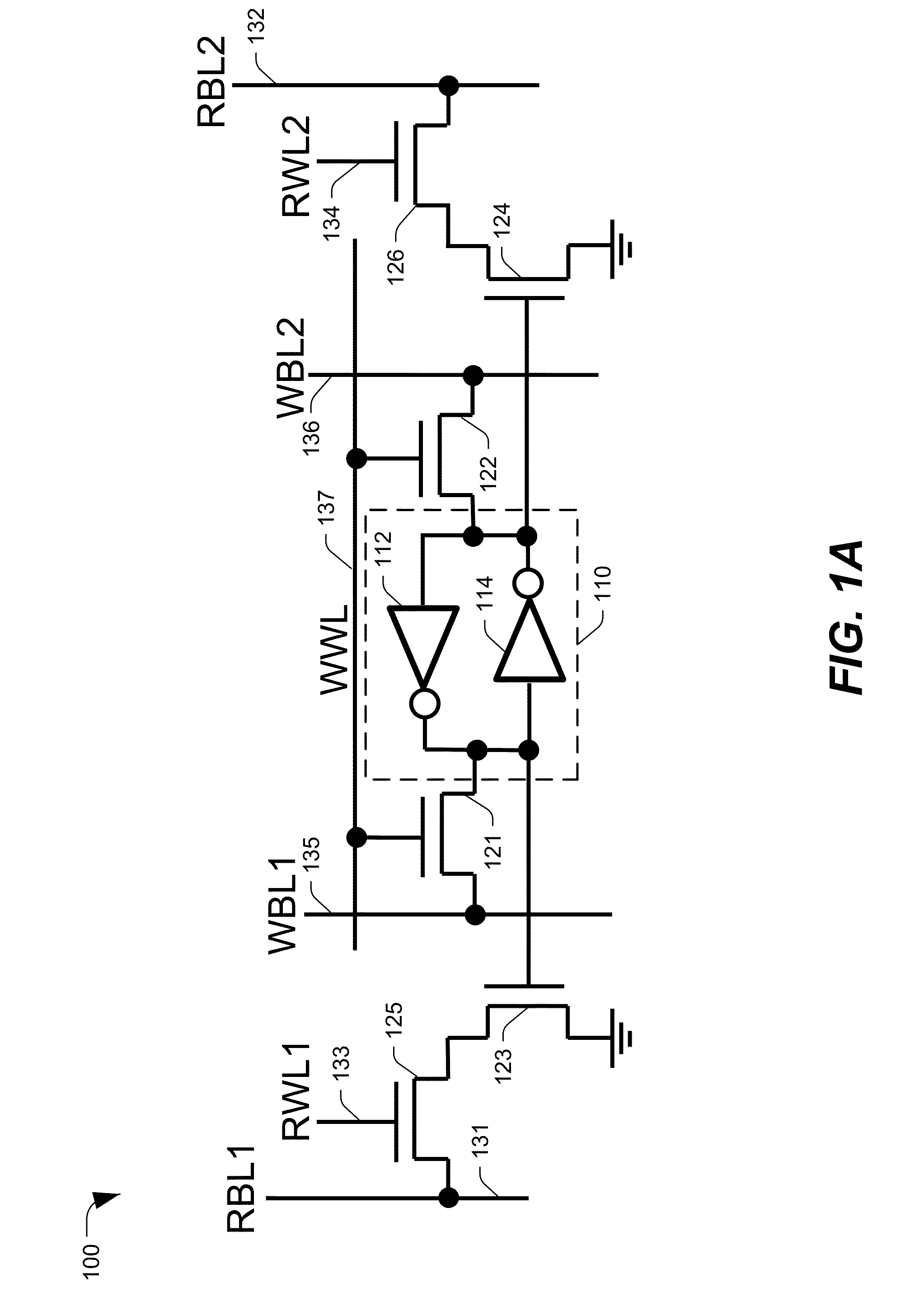
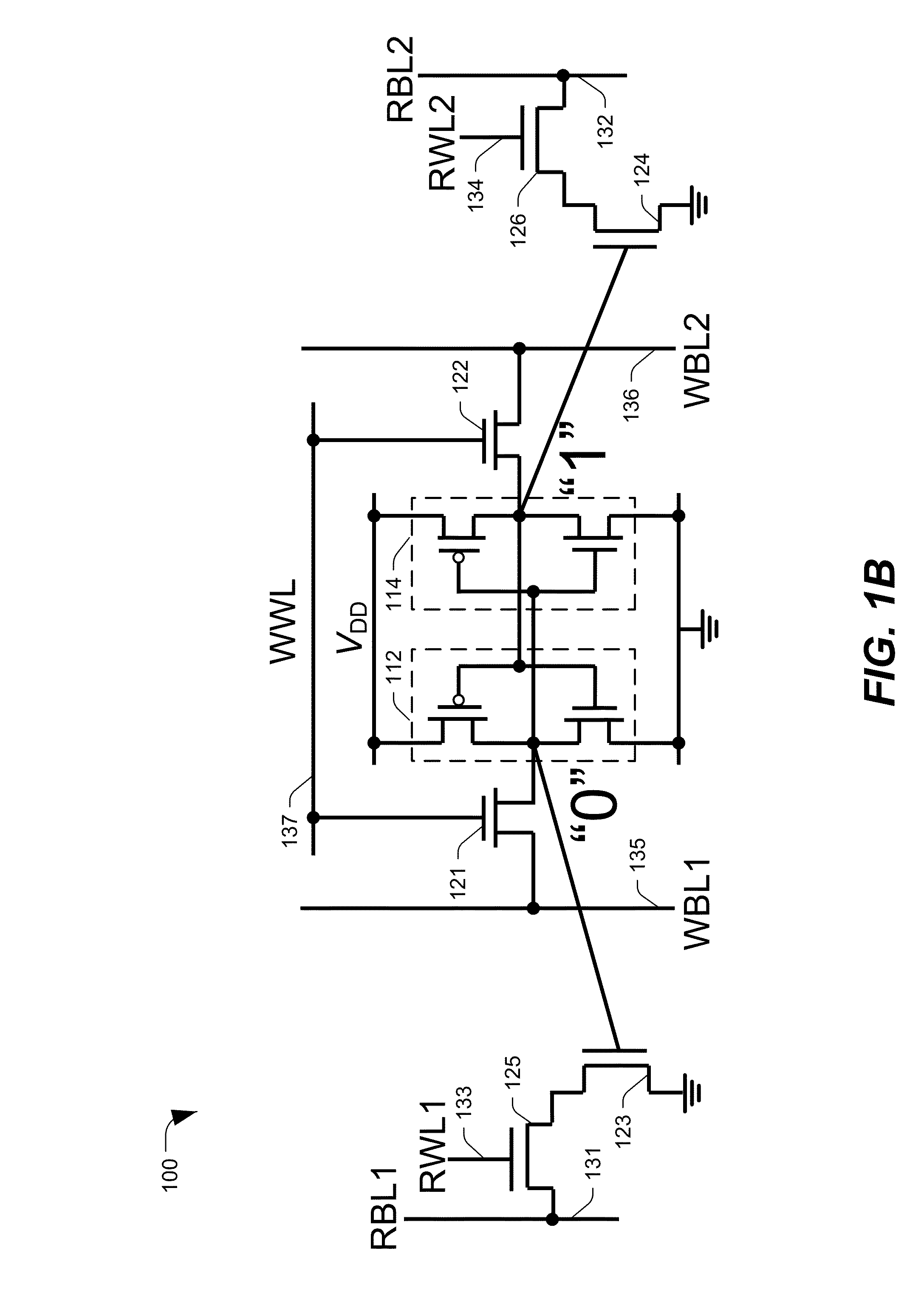
The present patent describes a design for a memory chip that includes multiple global word lines in a single metal layer. This design allows for better routing between different components within the chip and decreases read / write latency due to smaller word line resistive-capacitive (RC) impedance. The global word lines are placed across the width of two bit cells, which can be selected by row select logic. The technical effect of this design is improved performance and efficiency of the memory chip.

Problems solved by technology

However, SADP may not support non-linear patterns that include jogs.

Method used


Image

  • Shared global read and write word lines
  • Shared global read and write word lines
  • Shared global read and write word lines

Examples


Embodiment Construction

[0017]Scaling down from 14 nm technology may present challenges. For example, for technology nodes 14 nm and larger, the width of a 3-port bit cell may be restricted to being less than or equal to twice contacted poly pitch (CPP, the distance between contacted poly (gate) lines). For 14 nm, CPP may be approximately 80-90 nm. As used herein, cell “width” may be perpendicular to a poly direction and along a fin direction. For technology nodes smaller than 14 nm, CPP is reduced, which results in decreased bit cell width (e.g., a bit cell width of approximately 132 nm). When the bit cell width is reduced (i.e., narrowed), write and read word lines in the bit cell may also be narrowed, resulting in increased read / write latency due to increased word line resistor-capacitor (RC) impedance.

[0018]In conventional bit cells, global word lines may be located in a fourth metal layer (M4), a sixth metal layer (M6), and an eighth metal layer (M8). For example, each global word line may have a widt...


PUM


Abstract

An apparatus includes an array of bit cells that include a first row of bit cells and a second row of bit cells. The apparatus also includes a first global read word line configured to be selectively coupled to the first row of bit cells and to the second row of bit cells. The apparatus further includes a second global read word line configured to be selectively coupled to the first row of bit cells and to the second row of bit cells. The apparatus also includes a global write word line configured to be selectively coupled to the first row of bit cells and to the second row of bit cells. The first global read word line, the second global read word line, and the global write word line are located in a common metal layer.

Description

I. FIELD[0001]The present disclosure is generally related to read and write word lines for bit cells.II. DESCRIPTION OF RELATED ART[0002]Advances in technology have resulted in smaller and more powerful computing devices. For example, there currently exist a variety of portable personal computing devices, including wireless telephones, such as mobile and smart phones, tablets, and laptop computers, which are small, lightweight, and easily carried by users. These devices can communicate voice and data packets over wireless networks. Further, many such devices incorporate additional functionalities such as a digital still camera, a digital video camera, a digital recorder, and an audio file player. Also, such devices can process executable instructions, including software applications, such as a web browser application, that can be used to access the Internet. As such, these devices can include significant computing capabilities.[0003]Electronic devices, such as wireless telephones, m...

Claims


Application Information

Patent Timeline
IPC IPC(8): G11C11/419
CPCG11C11/419G11C8/14H01L27/0688G11C8/16H10B10/12
Inventor MOJUMDER, NILADRI NARAYANSONG, STANLEY SEUNGCHULWANG, ZHONGZELIU, PINGRIM, KERNYEAP, CHOH FEI
Owner QUALCOMM INC
Learn More