

Circuit board with embedded passive component and manufacturing method thereof
a passive component and circuit board technology, applied in the field of circuit boards, can solve the problems of space occupation, additional costs incurred by packaging, and the complexity of the semiconductor devi
- Summary
- Abstract
- Description
- Claims
- Application Information
AI Technical Summary
Benefits of technology
Problems solved by technology
Method used
Image

Examples
Embodiment Construction
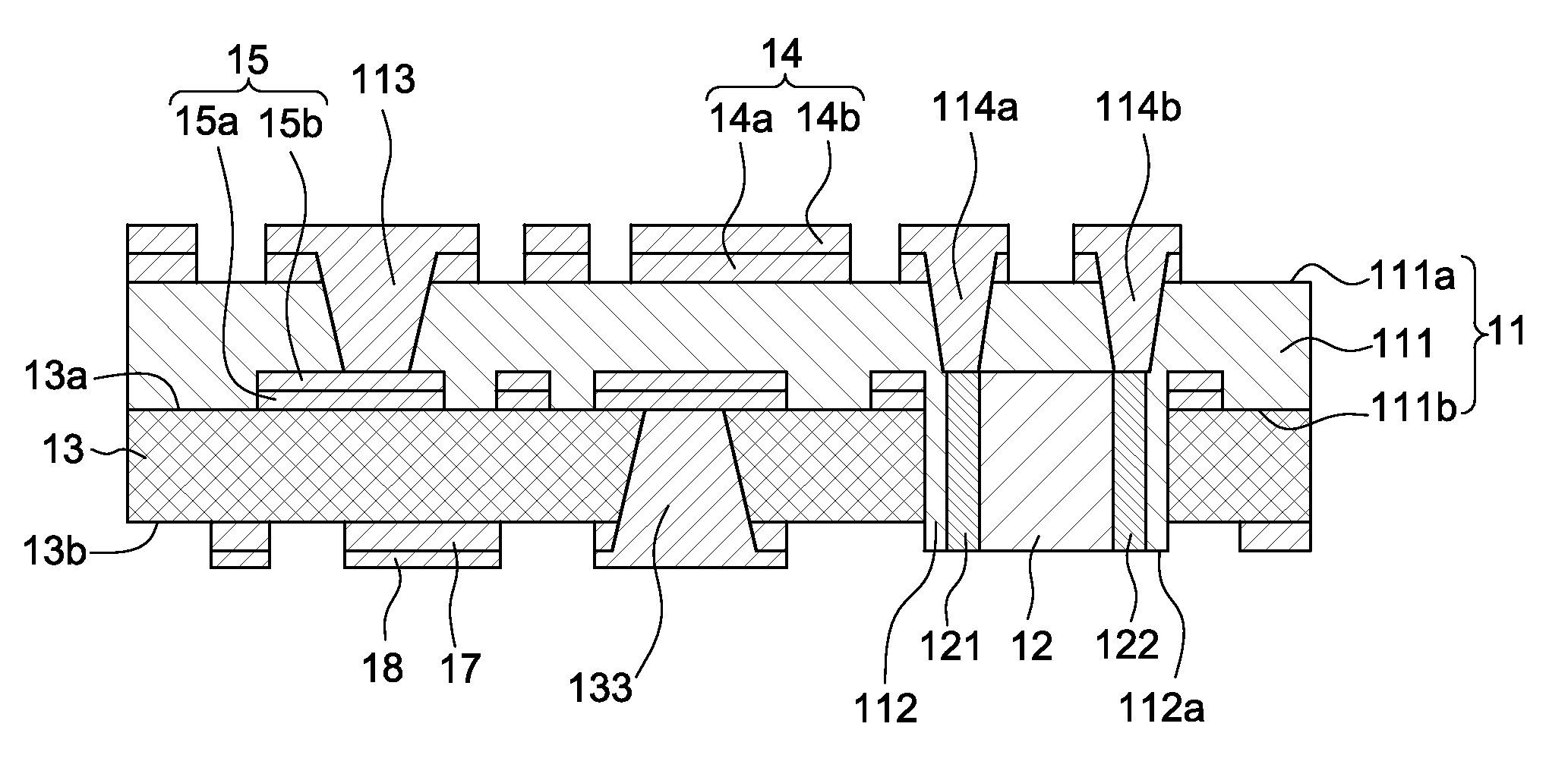
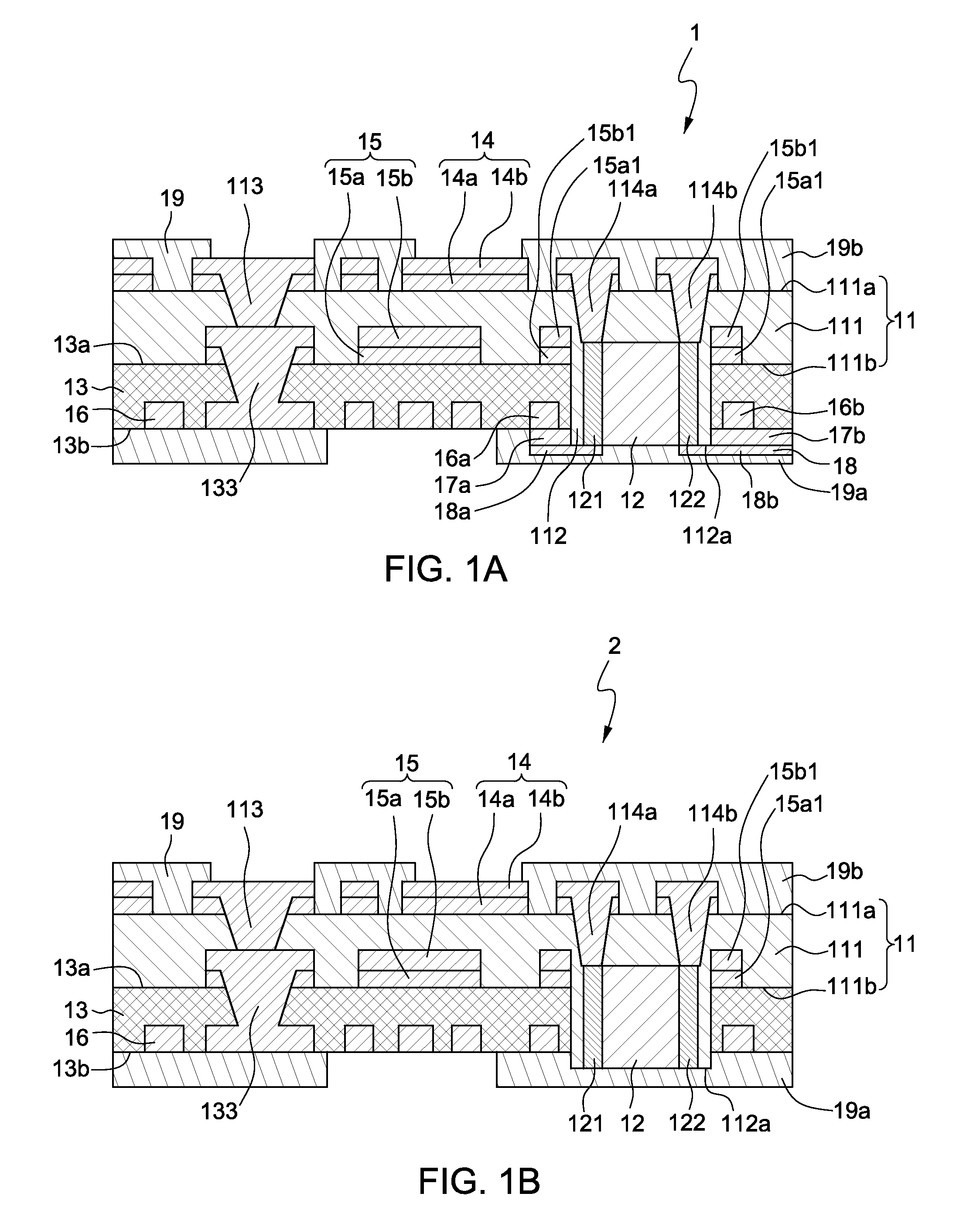
[0016]Various substrates having semiconductor devices embedded, so-called chip-embedded substrates, have been proposed, wherein an electronic device is first buried in a substrate and then a rerouting structure is fabricated in subsequent processes. The rerouting structure may include a redistribution layer (RDL) and interconnects (e.g., conducting posts) extending from the RDL and terminating as contact structures at the surface of a thick support layer, for the next level packaging structure. The RDL may be supported by the passivation layer formed over the embedded semiconductor device. A polymeric layer may be deposited over the RDL, and etched or drilled to provide a via for over-filling with a metal to form an interconnect (i.e., a conducting post) that extends above and beyond the opening of the via. A solder bump attached to the protruding end of the post may be formed by electroless plating, screen or stencil printing.
[0017]The top surface of the passivation layer may not b...
PUM
 Abstract
Description
Claims
Application Information