
Fingerprint identification chip with enhanced ESD protection

a fingerprint identification and protection circuit technology, applied in the field of fingerprint identification systems, can solve the problems of static electricity entering the esd protection circuit of the conventional fingerprint identification chip is usually too late to be activated, and the large transient current damage the chip, etc., to achieve the effect of enhancing the esd protection capability of the fingerprint identification chip

Active Publication Date: 2016-06-02
EGALAX EMPIA TECH INC
View PDF6 Cites 8 Cited by
  • Summary
  • Abstract
  • Description
  • Claims
  • Application Information

AI Technical Summary

Benefits of technology

The present invention is about a fingerprint identification chip that has better protection against high static electricity levels. The chip has receiving pads with a cavity in the middle and a raised edge around it. When a finger touches the chip, static electricity can escape through the edges to the ground, which makes the chip more resistant to damage. Overall, this design improves the reliability and durability of the fingerprint identification chip.

Problems solved by technology

Static electricity of human body or machine into a chip may generate large transient current that damages the chip.
However, the ESD protection circuit of conventional fingerprint identification chips is usually too late to be activated, such that static electricity may enter, malfunction or even damage internal circuitry of the chips.
Moreover, the ESD protection circuit of conventional fingerprint identification chips is ordinarily not strong enough, such that large electrostatic discharge may cause breakdown to the ESD protection circuit and deprive the internal circuitry of ESD protection.

Method used


Image

  • Fingerprint identification chip with enhanced ESD protection
  • Fingerprint identification chip with enhanced ESD protection
  • Fingerprint identification chip with enhanced ESD protection

Examples


Embodiment Construction

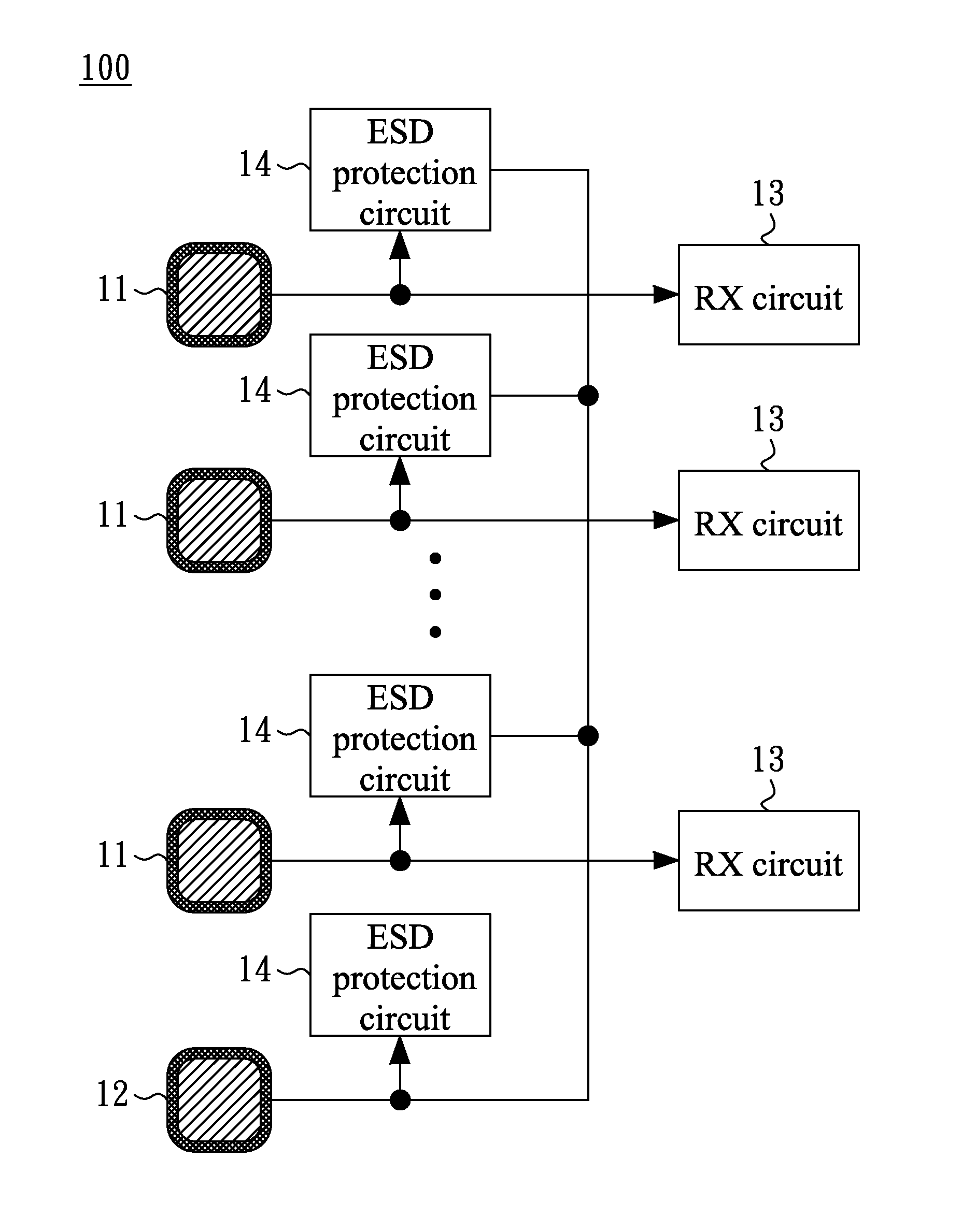
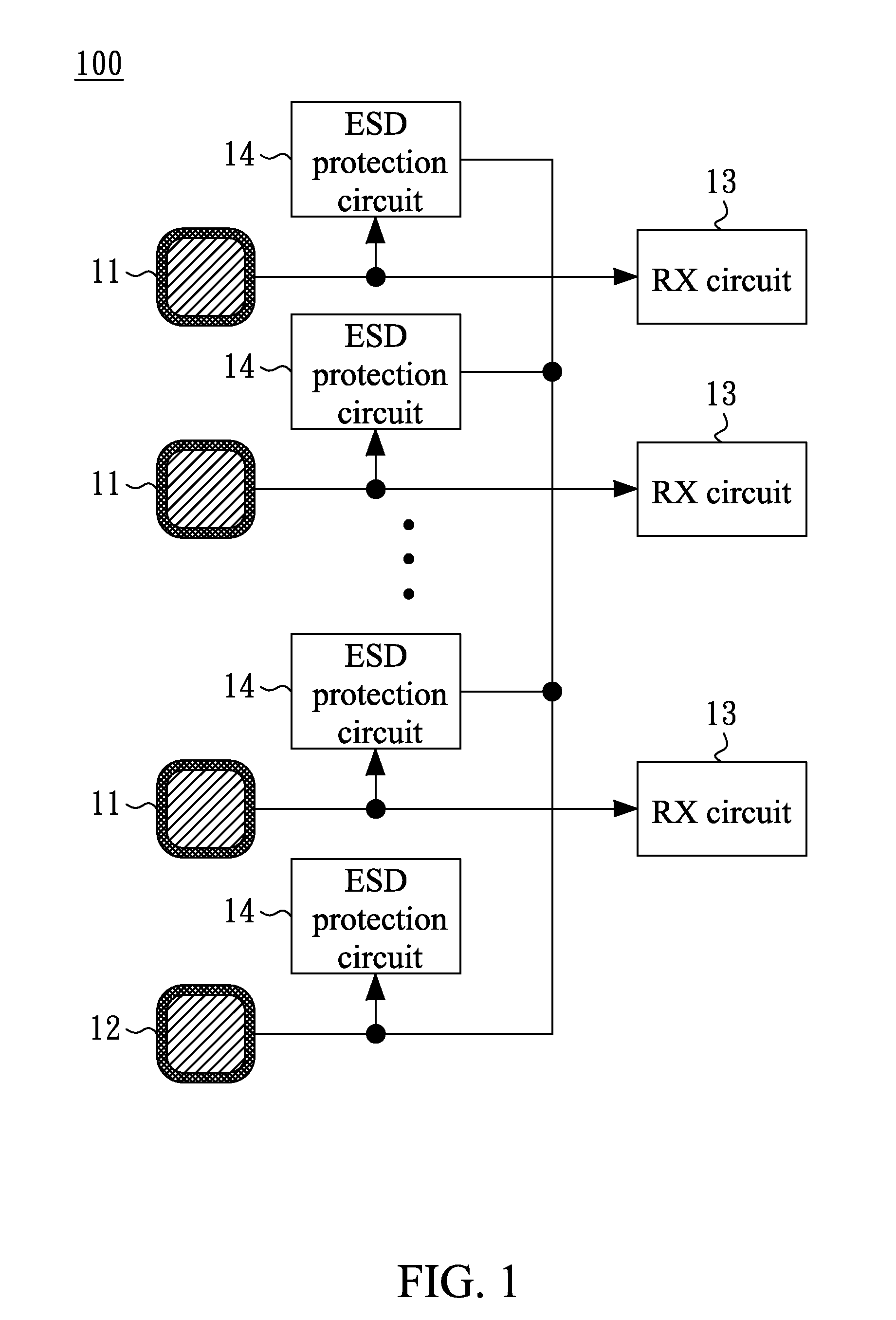
[0016]FIG. 1 shows a block diagram illustrated of a fingerprint identification system 100, which includes a plurality of receiving pads 11 and at least one power pad 12. The fingerprint identification system 100 also includes receiving (RX) circuits 13, which are electrically coupled to the receiving pads 11, respectively, for detecting fingerprint. The fingerprint identification system 100 further includes electrostatic discharge (ESD) protection circuits 14, which are electrically coupled to the receiving pads 11 and the power pad 12, for protecting the RX circuits 13 and internal circuitry (not shown).

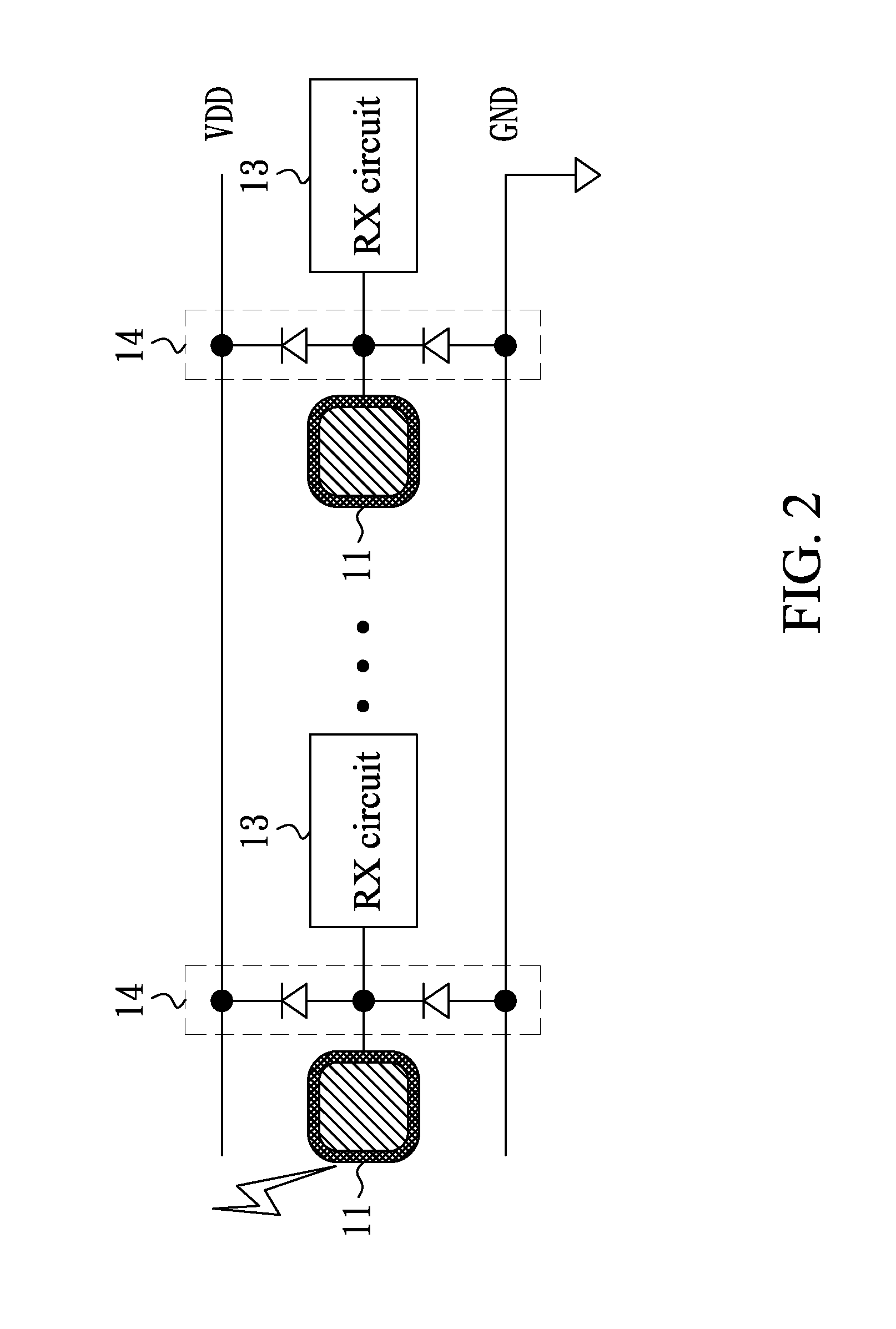
[0017]FIG. 2 shows a portion of the fingerprint identification system 100 of FIG. 1 for the purpose of demonstrating working principle of the fingerprint identification system 100. At the moment when a finger touches the receiving pad 11, static electricity of the finger with an amount greater than a predefined value may activate the ESD protection circuit 14 via the receiving pad 1...


PUM


Abstract

A fingerprint identification chip with enhanced ESD protection includes receiving pads disposed on a surface of a chip and arranged in a matrix format. The receiving pad has a central region and a peripheral region which surrounds at least an edge of the central region. The peripheral region of the receiving pad is higher than the central region.

Description

BACKGROUND OF THE INVENTION[0001]1. Field of the Invention[0002]The present invention generally relates to a fingerprint identification system, and more particularly to a fingerprint identification chip with enhanced electrostatic discharge (ESD) protection.[0003]2. Description of Related Art[0004]Fingerprint identification has been gradually used in electronic devices, particularly handheld electronic devices (e.g., mobile phones or tablet personal computers) to replace password identification in a more convenient and safer manner.[0005]Static electricity of human body or machine into a chip may generate large transient current that damages the chip. Electrostatic discharge (ESD) protection is thus an essential and important function for the chips. As the surface of a fingerprint identification chip is frequently subjected to finger touch, it thus needs more ESD protection capability than a general integrate circuit chip to ensure normal operation of the fingerprint identification....

Claims


Application Information

Patent Timeline
Patent Type & Authority Applications(United States)
IPC IPC(8): G06K9/00
CPCG06K9/00013G06V40/1329
Inventor LIN, PO-CHUAN
Owner EGALAX EMPIA TECH INC
Learn More