
Display Device and Driving Module thereof

a technology of display device and driving module, which is applied in the direction of static indicating devices, instruments, etc., can solve the problems of limited eye recognition ability and difficulty for users to recognize distances between pixels of lcd, and achieve the reduction of the number of sub-pixels for realizing the display device, power consumption and the layout area of the display device. , the effect of improving the number of sub-pixels

Active Publication Date: 2016-06-02
NOVATEK MICROELECTRONICS CORP
View PDF3 Cites 8 Cited by
  • Summary
  • Abstract
  • Description
  • Claims
  • Application Information

AI Technical Summary

Benefits of technology

The present invention provides a method for improving the aperture ratio and brightness of a display device by arranging sub-pixels in a specific way. By using this method, the display device can achieve better performance in terms of brightness and aperture ratio. Additionally, a driving module for the display device is also provided to further improve the aperture ratio and brightness. The sub-pixels are arranged in columns, with the first sub-pixel located at the first column, the second sub-pixel located at the second column, and so on. The height of each sub-pixel is different from the others, which helps to improve the aperture ratio and brightness of the display device. Overall, this invention provides a more efficient and effective way to improve the performance of display devices.

Problems solved by technology

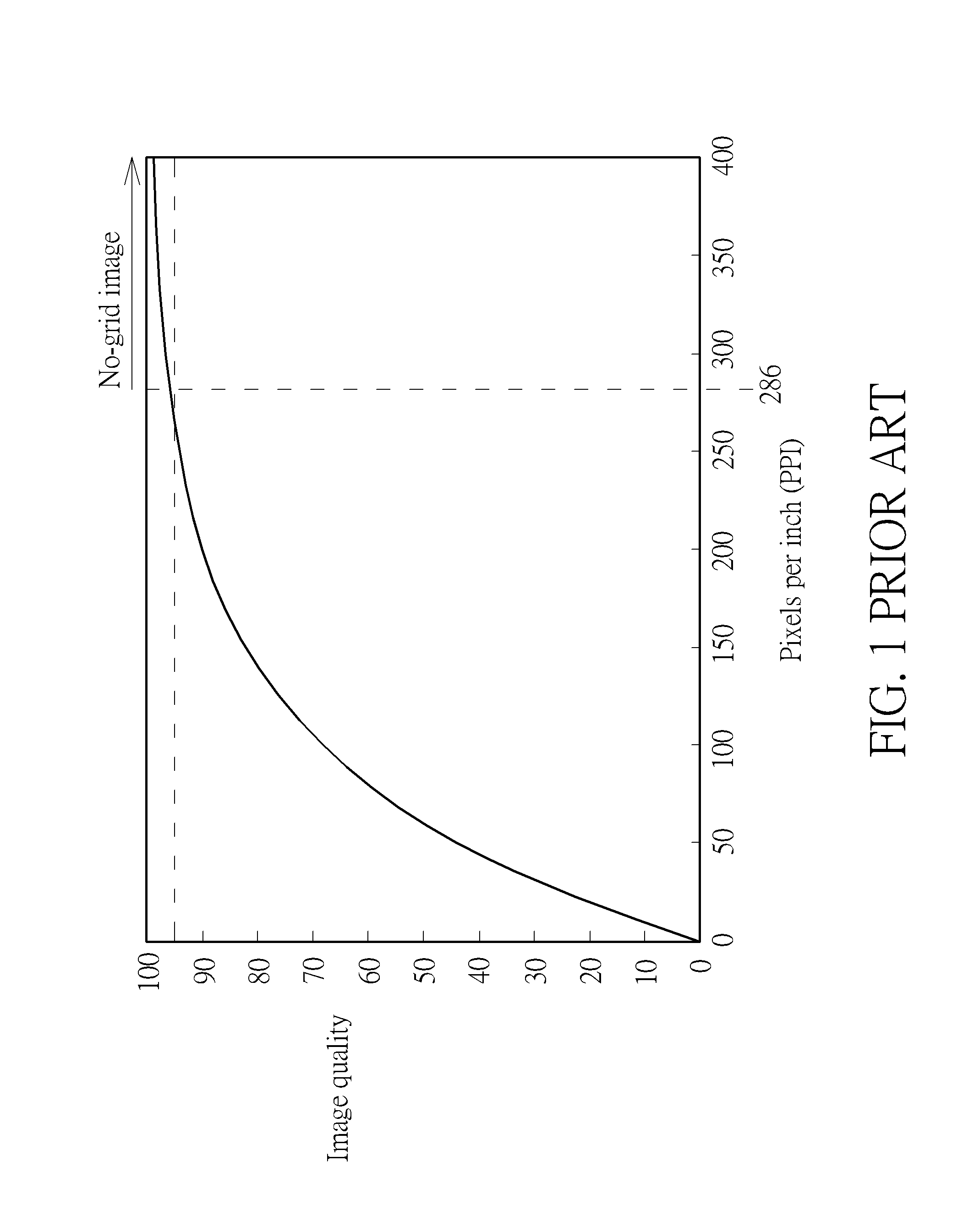
However, recognizing ability of the eyes has a limit.
For example, under a condition that the visual acuity of the user is 1.0 and a distance between the eyes and the LCD is 12 inches, it may be difficult for the user to recognize distances between the pixels of the LCD when the PPI of the LCD exceeds 286.

Method used


Image

  • Display Device and Driving Module thereof
  • Display Device and Driving Module thereof
  • Display Device and Driving Module thereof

Examples


Embodiment Construction

[0053]The present invention reduces a number of sub-pixels corresponding to each pixel via different arrangements of the sub-pixels. An aperture ratio and brightness of the liquid crystal display (LCD) are accordingly improved. The power consumption and the layout area of the LCD are further decreased.

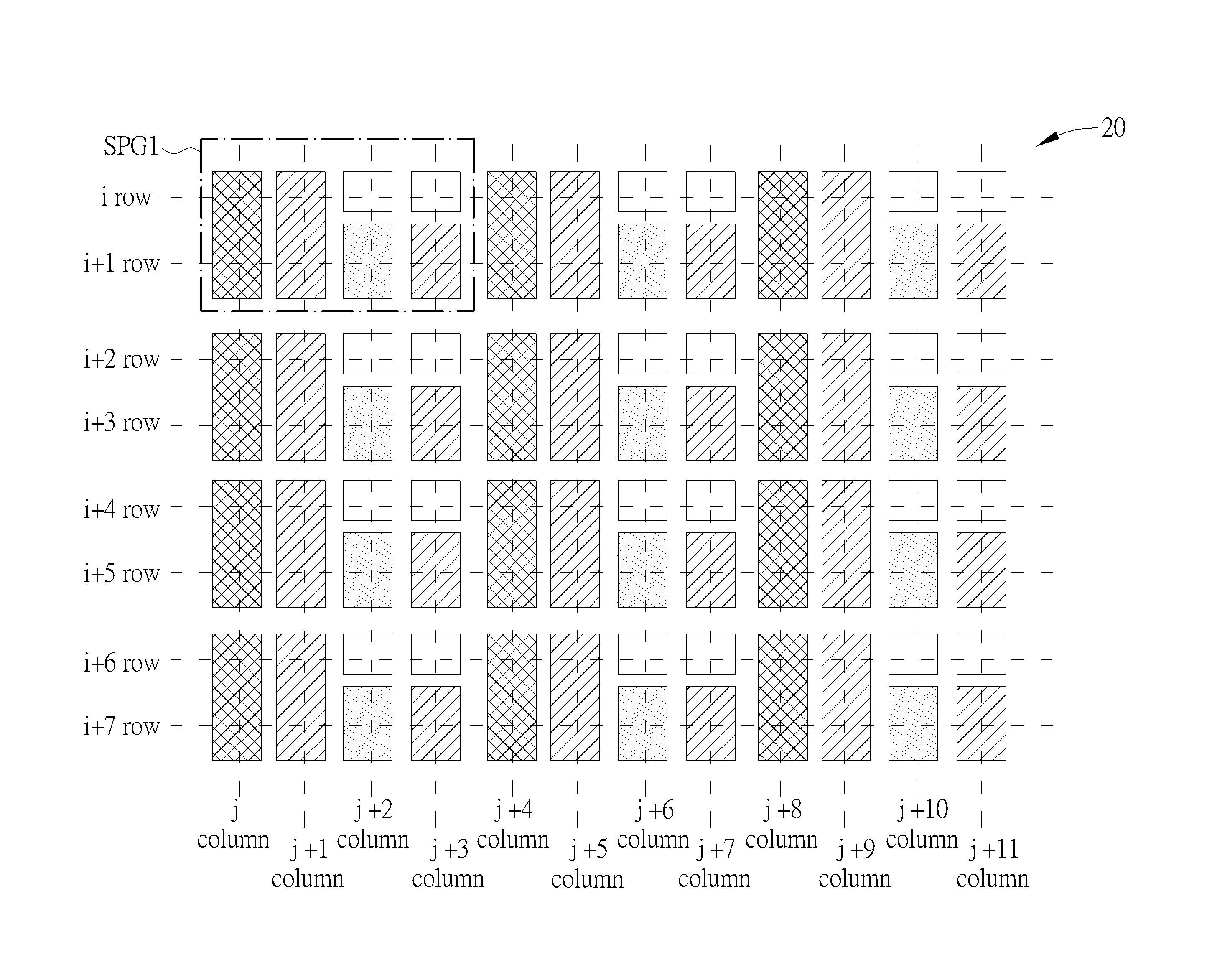
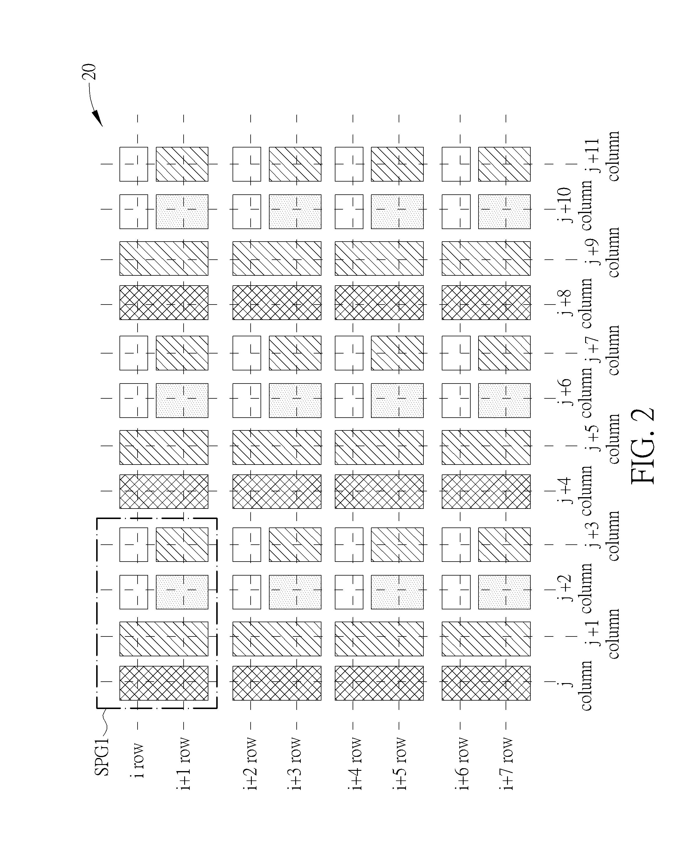
[0054]Please refer to FIG. 2, which is a schematic diagram of a display device 20 according to an example of the present invention. The display device 20 may be an electronic product with a liquid crystal panel, such as a television, a smart phone or a tablet, and is not limited herein. FIG. 2 only shows parts of sub-pixels of the display device 20 for illustrations. Note that, FIG. 2 is utilized for illustrating the relative positions of the sub-pixels and not for limiting the ratio between length and width. As shown in FIG. 2, the display device 20 comprises a plurality of repeatedly arranged sub-pixel groups SPG1 (only one sub-pixel group SPG1 is marked in FIG. 2 for illustrations)....


PUM


Abstract

A display device includes a plurality of sub-pixel groups. Each sub-pixel group includes a first sub-pixel located at a first column; a second sub-pixel located at a second column adjacent to the first column; a third sub-pixel located a third column adjacent to the second column; a fourth sub-pixel located at the third column; a fifth sub-pixel located at a fourth column adjacent to the third column; and a six sub-pixel located at the fourth column; wherein height of the first sub-pixel is different from or / equal to height of the second sub-pixel, a sum of heights of the third sub-pixel and the fourth sub-pixel, and a sum of heights of the fifth sub-pixel and the sixth sub-pixel; wherein height of the third sub-pixel is different from or equal to height of the fourth sub-pixel; wherein height of the fifth sub-pixel is different from or equal to height of sixth sub-pixel.

Description

BACKGROUND OF THE INVENTION[0001]1. Field of the Invention[0002]The present invention relates to a display device and driving module thereof, and more particularly, to a display device reducing power consumption and increasing brightness via changing sub-pixel arrangement method and driving module thereof.[0003]2. Description of the Prior Art[0004]A liquid crystal display (LCD) is a flat panel display which has the advantages of low radiation, light weight and low power consumption and is widely used in various information technology (IT) products, such as notebook computers, personal digital assistants (PDA), and mobile phones. An active matrix thin film transistor (TFT) LCD is the most commonly used transistor type in LCD families, and particularly in the large-size LCD family. A driving system installed in the LCD includes a timing controller, source drivers and gate drivers. The source and gate drivers respectively control data lines and scan lines, which intersect to form a cel...

Claims


Application Information

Patent Timeline
Patent Type & Authority Applications(United States)
IPC IPC(8): G09G3/36
CPCG09G3/3611G09G2330/021G09G2320/0233
Inventor YANG, KAI-MINPAI, FENG-TING
Owner NOVATEK MICROELECTRONICS CORP
Learn More