
Non-lithographically patterned directed self assembly alignment promotion layers

Active Publication Date: 2016-06-16
INTEL CORP
View PDF0 Cites 9 Cited by
  • Summary
  • Abstract
  • Description
  • Claims
  • Application Information

AI Technical Summary

Benefits of technology

This patent is about a method for making very small interconnect structures in integrated circuits. The method addresses challenges that arise when patterning extremely small interconnect structures using lithographic processes. The invention proposes a method that uses a block copolymer molecule to promote positioning or alignment of assembled structures during self-assembly. The method also addresses the challenge of controlling the overlay between vias and interconnects, as well as the challenge of maintaining the same overall fraction of the critical dimension budget as the critical dimensions decrease in photoresists. The technical effects of the invention include improved precision in the patterning of very small interconnect structures and improved quality of the finished product.

Problems solved by technology

When patterning extremely small interconnect structures and / or interconnect structures at extremely small pitches by such lithographic processes, several challenges tend to present themselves, especially when the pitches are around 50 nanometers (nm) or less and / or when the critical dimensions of the lines and / or vias are around 20 nm or less.
One potential challenge is that the overlay between the vias and the overlying interconnects, and the overlay between the vias and the underlying landing interconnects, generally need to be controlled to high tolerances.
Another potential challenge is that the critical dimensions of the openings (e.g., the via openings) generally tend to scale faster than the resolution capabilities of the lithographic scanners.
However, the shrink amount tends to be limited by the minimum pitch, as well as by the ability of the shrink process to be sufficiently optical proximity correction (OPC) neutral, and to not significantly compromise line width roughness (LWR) and / or critical dimension uniformity (CDU).
Yet another potential challenge is that the LWR and / or CDU characteristics of photoresists generally need to improve as the critical dimensions decrease in order to maintain the same overall fraction of the critical dimension budget.
However, currently the LWR and / or CDU characteristics of most photoresists are not improving as rapidly as the critical dimensions are decreasing.

Method used


Image

  • Non-lithographically patterned directed self assembly alignment promotion layers
  • Non-lithographically patterned directed self assembly alignment promotion layers
  • Non-lithographically patterned directed self assembly alignment promotion layers

Examples


example embodiments

[0091]The following examples pertain to further embodiments. Specifics in the examples may be used anywhere in one or more embodiments.

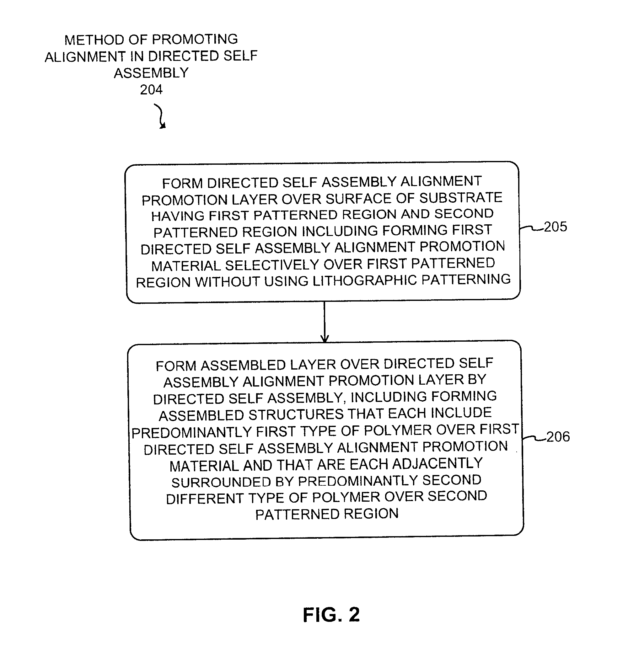
[0092]Example 1 is a fabrication method including forming a directed self assembly alignment promotion layer over a surface of a substrate having a first patterned region and a second patterned region. The forming of the directed self assembly alignment promotion layer includes forming a first directed self assembly alignment promotion material selectively over the first patterned region. The forming of the first directed self assembly alignment promotion material selectively over the first patterned region is optionally performed without using lithographic patterning. The method also includes forming an assembled layer over the directed self assembly alignment promotion layer by directed self assembly. The forming of the assembled layer including forming a plurality of assembled structures that each include predominantly a first type of polymer over...


PUM


Abstract

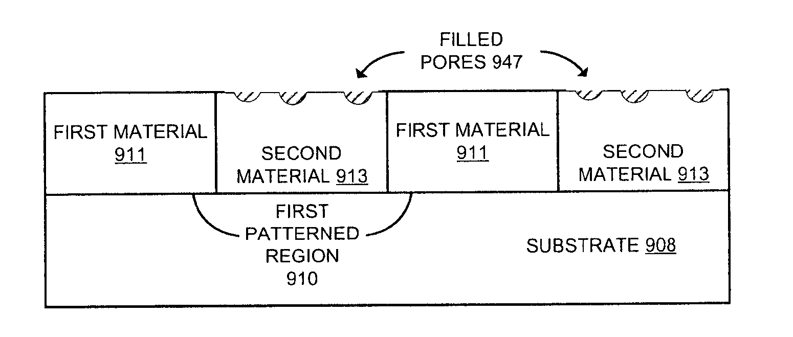
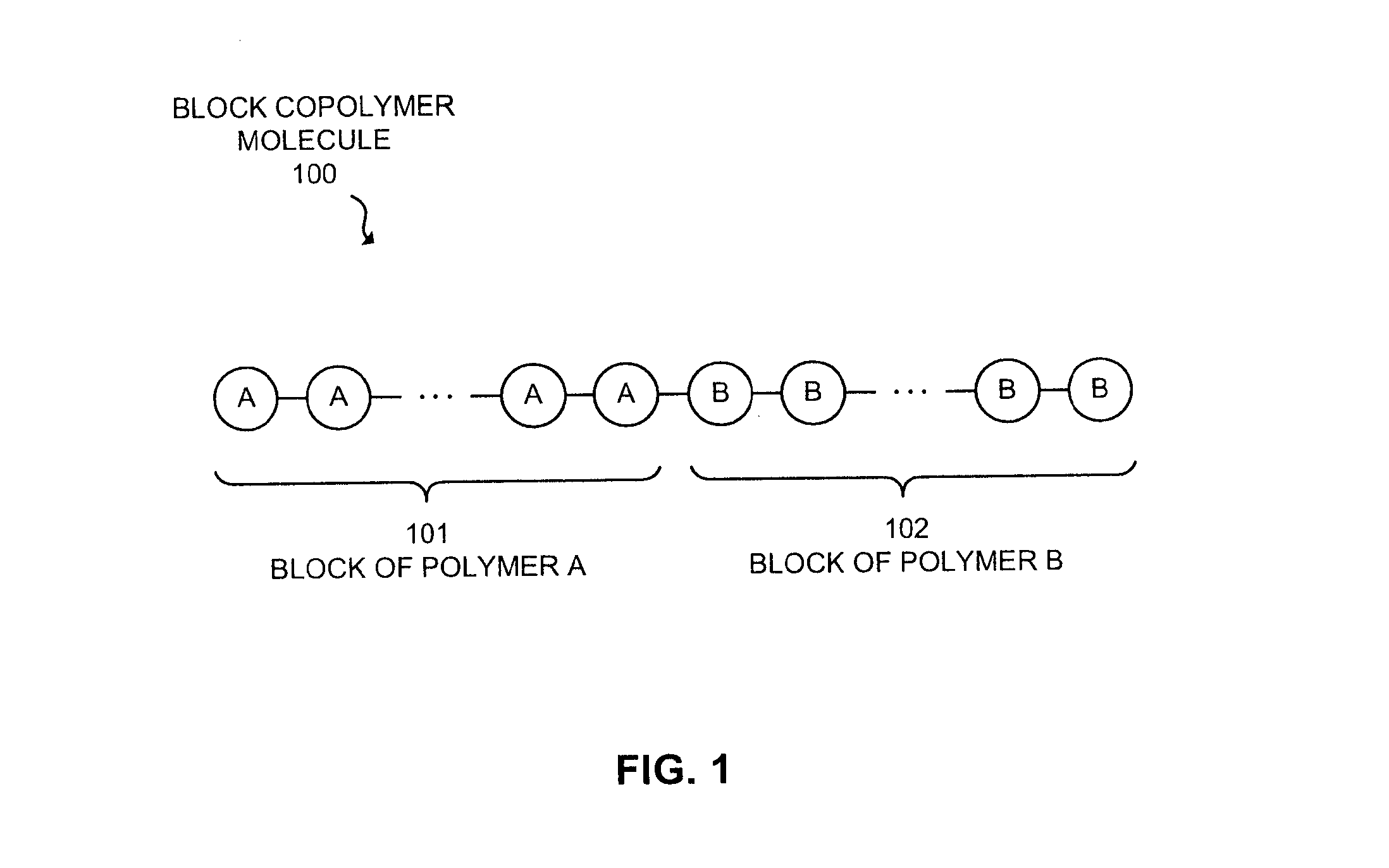
A method of an aspect includes forming a directed self assembly alignment promotion layer over a surface of a substrate having a first patterned region and a second patterned region. A first directed self assembly alignment promotion material is formed selectively over the first patterned region without using lithographic patterning. The method also includes forming an assembled layer over the directed self assembly alignment promotion layer by directed self assembly. A plurality of assembled structures are formed that each include predominantly a first type of polymer over the first directed self assembly alignment promotion material. The assembled structures are each adjacently surrounded by predominantly a second different type of polymer over the second patterned region. The first directed self assembly alignment promotion material has a greater chemical affinity for the first type of polymer than for the second different type of polymer.

Description

[0001]This application is a U.S. National Phase application under 35 U.S.C. §371 of International Application No. PCT / US2013 / 048307, filed Jun. 27, 2013.BACKGROUND[0002]1. Field[0003]Embodiments relate to the field of directed self assembly. In particular, embodiments relate to aligning or positioning structures formed through directed self assembly.[0004]2. Background Information[0005]Integrated circuits generally include interconnect structures to electrically couple circuitry formed in a semiconductor substrate (e.g., transistors and other circuit elements) with an external signaling medium (e.g., a package, pins, printed circuit board, etc.). Often multi-layer interconnect structures are employed that include multiple levels of generally coplanar metal or other interconnect lines disposed within a dielectric or insulating layer. Vias are generally used to provide select electrical couplings between interconnect lines on different levels by providing electrically conductive paths...

Claims


Application Information

Patent Timeline
IPC IPC(8): H01L21/768H01L23/532H01L23/528H01L21/02H01L21/311
CPCH01L21/76822H01L21/02118H01L23/5329H01L21/76834H01L23/528H01L21/31127H01L21/0271B81C1/00031B81C2201/0149H01L2924/0002H01L2924/00H01L21/02205H01L21/02299H01L21/02439H01L21/02658H01L21/768H01L21/31051H01L21/76897H01L23/5328
Inventor BRISTOL, ROBERT L.HOURANI, RAMIHAN, EUNGNAKBLACKWELL, JAMES M.
Owner INTEL CORP
Learn More